DS91M040
www.ti.com
SNLS283M – FEBRUARY 2008 – REVISED APRIL 2013
DS91M040 125 MHz Quad M-LVDS Transceiver
Check for ...
DS91M040
www.ti.com
SNLS283M – FEBRUARY 2008 – REVISED APRIL 2013
DS91M040 125 MHz Quad M-LVDS Transceiver
Check for Samples: DS91M040
FEATURES
1
2 DC - 125 MHz / 250 Mbps Low Jitter, Low Skew, Low Power Operation
Wide Input Common Mode
Voltage Range Allows up to ±1V of GND Noise
Conforms to TIA/EIA-899 M-LVDS Standard Pin Selectable M-LVDS Receiver Type (1 or 2) Controlled Transition Times (2.0 ns typ)
Minimize Reflections 8 kV ESD on M-LVDS I/O pins protects
adjoining components Flow-Through Pinout Simplifies PCB Layout Small 5 mm x 5 mm WQFN-32 Space Saving
Package
APPLICATIONS
Multidrop / Multipoint Clock and Data Distribution
High-Speed, Low Power, Short-Reach Alternative to TIA/EIA-485/422
Clock Distribution in AdvancedTCA (ATCA) and MicroTCA (μTCA, uTCA) Backplanes
DESCRIPTION
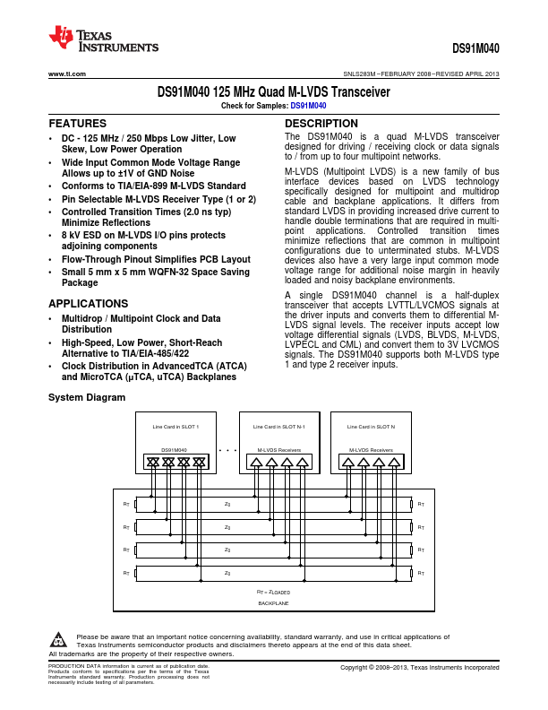
The DS91M040 is a quad M-LVDS transceiver designed for driving / receiving clock or data signals to / from up to four multipoint networks.
M-LVDS (Multipoint LVDS) is a new family of bus interface devices based on LVDS technology specifically designed for multipoint and multidrop cable and backplane applications. It differs from standard LVDS in providing increased drive current to handle double terminations that are required in multipoint applications. Controlled transition times minimize reflections that are common in multipoint configurations due to unterminated stubs. M-LVDS devices also have a very large input common mode
voltage range for additional noise margin in...