DMN2005LPK
Lead-free Green
N-CHANNEL ENHANCEMENT MODE FIELD EFFECT TRANSISTOR
NEW PRODUCT
Features
· · · · · · · ·
Lo...
DMN2005LPK
Lead-free Green
N-CHANNEL ENHANCEMENT MODE FIELD EFFECT TRANSISTOR
NEW PRODUCT
Features
· · · · · · · ·
Low On-Resistance Low Gate Threshold
Voltage Fast Switching Speed Low Input/Output Leakage Ultra-Small Surface Mount Package Lead Free By Design/RoHS Compliant (Note 2) "Green" Device (Note 4) ESD Protected Gate
UNDER DEVELOPMENT
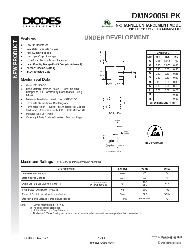
DFN1006-3
G H
Dim A
A K
Min 0.95 0.55 0.45 0.20 0.47 0 0.10 0.20 ¾ ¾
Max 1.075 0.675 0.55 0.30 0.53 0.05 0.20 0.30 ¾ ¾
Typ 1.00 0.60 0.50 0.25 0.50 0.03 0.15 0.25 0.35 0.40
B C D G H
B C
M
Mechanical Data
· · · · · · ·
Case: DFN1006-3 Case Material: Molded Plastic, “Green” Molding Compound. UL Flammability Classification Rating 94V-0 Moisture Sensitivity: Level 1 per J-STD-020C Terminals Connections: See Diagram Terminals: Finish ¾ Matte Tin annealed over Copper leadframe. Solderable per MIL-STD-202, Method 208 Marking: See Last Page Ordering & Date Code Information: See Last Page
Drain
D
N
L
K L M N
G D S
TOP VIEW
All Dimensions in mm
Body Diode Gate
Gate Protection Diode
ESD protected
Source
EQUIVALENT CIRCUIT
Maximum Ratings
Drain-Source
Voltage Gate-Source
Voltage
@ TA = 25°C unless otherwise specified Characteristic Symbol VDSS VGSS Continuous Pulsed (Note 3) ID Pd RqJA Tj, TSTG Value 20 ±8 200 250 200 625 -65 to +150 Units V V mA mW °C/W °C
Drain Current per element (Note 1) Total Power Dissipation (Note 1) Thermal Resistance, Junction to Ambient Operating and Storage Temperature Range
Note:
1. Device moun...