DM74AS30 8 Input NAND Gate
April 1984 Revised March 2000
DM74AS30 8 Input NAND Gate
General Description
This device co...
DM74AS30 8 Input NAND Gate
April 1984 Revised March 2000
DM74AS30 8 Input NAND Gate
General Description
This device contains a single gate which performs the logic NAND function.
Features
s Switching specifications at 50 pF s Switching specifications guaranteed over full temperature and VCC range s Advanced oxide-isolated, ion-implanted Schottky TTL process s Functionally and pin for pin compatible with Schottky, low power Schottky, and advanced low power Schottky TTL counterpart s Improved AC performance over Schottky, low power Schottky, and advanced low power Schottky counterparts
Ordering Code:
Order Number DM74AS30M DM74AS30N Package Number M14A N14A Package Description 14-Lead Small Outline Integrated Circuit (SOIC), JEDEC MS-012, 0.150 Narrow 14-Lead Plastic Dual-In-Line Package (PDIP), JEDEC MS-001, 0.300 Wide
Devices also available in Tape and Reel. Specify by appending the suffix letter “X” to the ordering code.
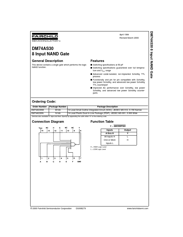
Connection Diagram
Function Table
Y = ABCDEFGH Inputs A thru H All inputs H One or More Inputs L
H = HIGH Logic Level L = LOW Logic Level
Output Y L H
© 2000 Fairchild Semiconductor Corporation
DS006279
www.fairchildsemi.com
DM74AS30
Absolute Maximum Ratings(Note 1)
Supply
Voltage Input
Voltage Operating Free Air Temperature Range Storage Temperature Range Typical θJA N Package M Package 84.0°C/W 114.0°C/W 7V 7V 0°C to +70°C −65°C to +150°C
Note 1: The “Absolute Maximum Ratings” are those values beyond which the safety of the device cannot be gu...