DM74ALS1032A Quadruple 2-Input OR Buffer
September 1986 Revised February 2000
DM74ALS1032A Quadruple 2-Input OR Buffer...
DM74ALS1032A Quadruple 2-Input OR Buffer
September 1986 Revised February 2000
DM74ALS1032A Quadruple 2-Input OR Buffer
General Description
These devices contain four independent buffers, each of which performs the logic OR function. The DM74ALS1032A is a buffer version of the DM74ALS32.
Features
s Switching specifications at 50 pF s Switching specifications guaranteed over full temperature and VCC range s Advanced oxide-isolated, ion-implanted Schottky TTL process s Improved line receiving characteristics
Ordering Code:
Order Number DM74ALS1032AM DM74ALS1032AN Package Number M14A N14A Package Description 14-Lead Small Outline Integrated Circuit (SOIC), JEDEC MS-012, 0.150 Narrow 14-Lead Plastic Dual-In-Line Package (PDIP), JEDEC MS-001, 0.300 Wide
Devices also available in Tape and Reel. Specify by appending the suffix letter “X” to the ordering code.
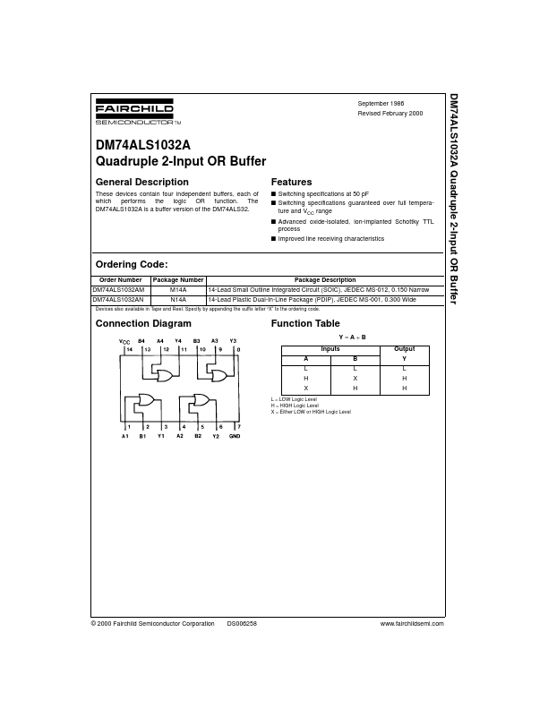
Connection Diagram
Function Table
Y=A+B Inputs A L H X
L = LOW Logic Level H = HIGH Logic Level X = Either LOW or HIGH Logic Level
Output B L X H Y L H H
© 2000 Fairchild Semiconductor Corporation
DS006258
www.fairchildsemi.com
DM74ALS1032A
Absolute Maximum Ratings(Note 1)
Supply
Voltage Input
Voltage Operating Free Air Temperature Range Storage Temperature Range Typical θJA N Package M Package 83.0°C/W 114.0°C/W 7V 7V 0°C to +70°C −65°C to +150°C
Note 1: The “Absolute Maximum Ratings” are those values beyond which the safety of the device cannot be guaranteed. The device should not be operated at these limits. The ...