8-Input Universal Shift/Storage Register with Common Parallel I/O Pins
DM54LS299 DM74LS299 8-Input Universal Shift Storage Register with Common Parallel I O Pins
June 1992
DM54LS299 DM74LS2...
Description
DM54LS299 DM74LS299 8-Input Universal Shift Storage Register with Common Parallel I O Pins
June 1992
DM54LS299 DM74LS299 8-Input Universal Shift Storage Register with Common Parallel I O Pins
General Description
The ’LS299 is an 8-bit universal shift storage register with TRI-STATE outputs Four modes of operation are possible hold (store) shift left shift right and load data The parallel load inputs and flip-flop outputs are multiplexed to reduce the total number of package pins Separate outputs are provided for flip-flops Q0 and Q7 to allow easy cascading A separate active LOW Master Reset is used to reset the register
Features
Y Y
Y
Y
Common I O for reduced pin count Four operation modes shift left shift right load and store Separate shift right serial input and shift left serial input for easy cascading TRI-STATE outputs for bus oriented applications
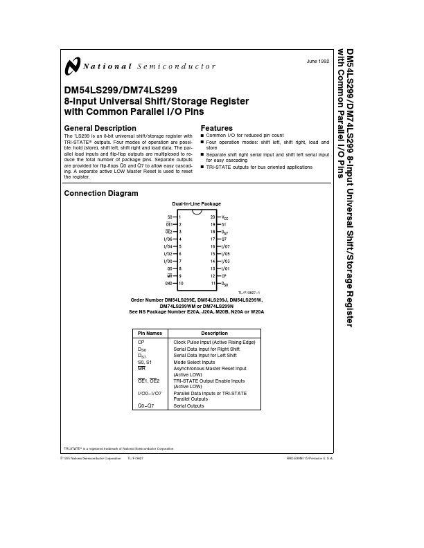
Connection Diagram
Dual-In-Line Package
TL F 9827 – 1
Order Number DM54LS299E DM54LS299J DM54LS299W DM74LS299WM or DM74LS299N See NS Package Number E20A J20A M20B N20A or W20A
Pin Names CP DS0 DS7 S0 S1 MR OE1 OE2 I O0–I O7 Q0–Q7
Description Clock Pulse Input (Active Rising Edge) Serial Data Input for Right Shift Serial Data Input for Left Shift Mode Select Inputs Asynchronous Master Reset Input (Active LOW) TRI-STATE Output Enable Inputs (Active LOW) Parallel Data Inputs or TRI-STATE Parallel Outputs Serial Outputs
TRI-STATE is a registered trademark of National Semiconductor Corporation C1995 National Semiconduct...
Similar Datasheet