DM54L04 Hex Inverting Gate
July 1989
DM54L04 Hex Inverting Gate
General Description
This device contains six independe...
DM54L04 Hex Inverting Gate
July 1989
DM54L04 Hex Inverting Gate
General Description
This device contains six independent gates each of which performs the logic INVERT function
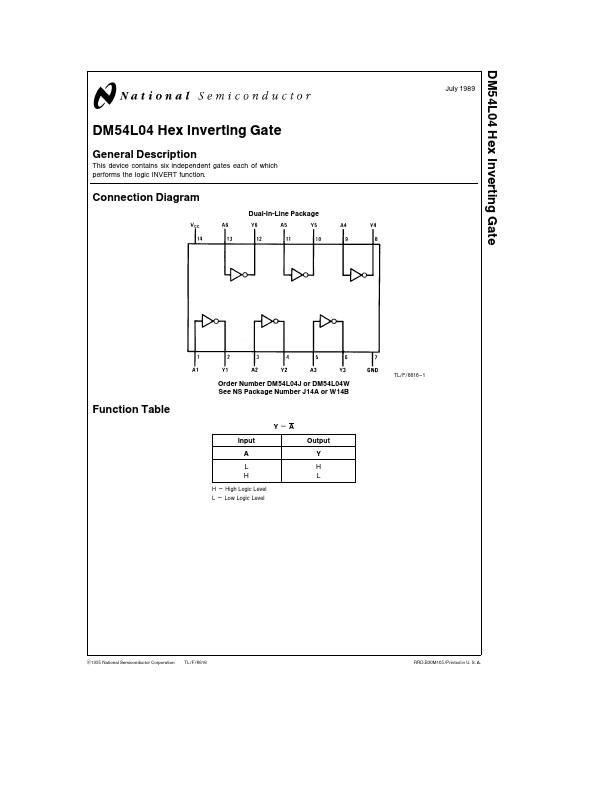
Connection Diagram
Dual-In-Line Package
TL F 6616 – 1
Order Number DM54L04J or DM54L04W See NS Package Number J14A or W14B
Function Table
YeA Input A L H
H e High Logic Level L e Low Logic Level
Output Y H L
C1995 National Semiconductor Corporation
TL F 6616
RRD-B30M105 Printed in U S A
Absolute Maximum Ratings (Note)
If Military Aerospace specified devices are required please contact the National Semiconductor Sales Office Distributors for availability and specifications Supply
Voltage 8V Input
Voltage 5 5V Operating Free Air Temperature Range b 55 C to a 125 C DM54L b 65 C to a 150 C Storage Temperature Range Note The ‘‘Absolute Maximum Ratings’’ are those values beyond which the safety of the device cannot be guaranteed The device should not be operated at these limits The parametric values defined in the ‘‘Electrical Characteristics’’ table are not guaranteed at the absolute maximum ratings The ‘‘Recommended Operating Conditions’’ table will define the conditions for actual device operation
Recommended Operating Conditions
Symbol VCC VIH VIL IOH IOL TA Parameter Min Supply
Voltage High Level Input
Voltage Low Level Input
Voltage High Level Output Current Low Level Output Current Free Air Operating Temperature
b 55
DM54L04 Nom 5 Max 55
Units V V 07
b0 2
45 2
V mA mA C
2 125
Electric...