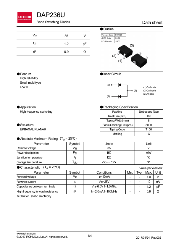
DAP236U
Diodes
Band switching diode
DAP236U
!Applications High speed switching !External dimensions (Units : mm)
DAP236...
DAP236U
Diodes
Band switching diode
DAP236U
!Applications High speed switching !External dimensions (Units : mm)
DAP236U
2.0±0.2 1.3±0.1 0.65 0.65 0.3 0.9±0.1 0.6
0.3±0.1
0.15±0.05
(All leads have the same dimensions)
!Construction Silicon epitaxial planar
ROHM : UMD3 EIAJ : SC-70 JEDEC : SOT-323
!Circuit
!Absolute maximum ratings (Ta=25°C)
Parameter
DC reverse
voltage Power dissipation Junction temperature Storage temperature
Symbol VR P Tj Tstg
Limits 35 150 125 −55∼+125
Unit V mW ˚C ˚C
!Electrical characteristics (Ta=25°C)
Parameter
Forward
voltage Reverse current Capacitance between terminals Forward operating resistance
Symbol VF IR CT rF
Min. − − − −
Typ. − − − −
Max. 1.0 10 1.2 0.90
Unit V nA pF Ω IF=10mA VR=25V
Conditions
VR=6V, f=1MHz IF=2mA, f=100MHz
0.1Min.
X
!Features 1) Multiple diodes with common anode configuration. (UMD3) 2) High reliability.
1.25±0.1
2.1±0.1
0∼0.1
DAP236U
Diodes
!Electrical characteristic curves (Ta=25°C)
1
FORWARD CURRENT : IF(mA)
REVERSE CURRENT : IR (nA)
10.0
CAPACITANCE BETWEEN TERMINALS : CT (pF)
10 20 30 40 50
3
100m 10m 1m 100µ 10µ 1µ 100n 0.4
2
1.0
1
0.5
0.6
0.7
0.8
0.9
1.0
1.1
0.1 0
0 0
10
20
30
FORWARD
VOLTAGE : VF (V)
REVERSE
VOLTAGE : VR (V)
REVERSE
VOLTAGE : VR (V)
Fig. 1 Forward characteristics
Fig. 2 Reverse characteristics
Fig. 3 Capacitance between terminals characteristics
FORWARD OPERATING RESISTANCE : rF (Ω)
1.0 f=100MHz
0.5
0.2
0 1
2
5
10
FORWARD CURRENT : IF (mA...