1-Mbit (64K x 18) Flow-Through Sync SRAM
CY7C1297F
1-Mbit (64K x 18) Flow-Through Sync SRAM
Features
• 64K x 18 common I/O • 3.3V –5% and +10% core power supply...
Description
CY7C1297F
1-Mbit (64K x 18) Flow-Through Sync SRAM
Features
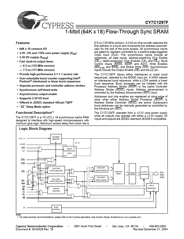
64K x 18 common I/O 3.3V –5% and +10% core power supply (VDD) 3.3V I/O supply (VDDQ) Fast clock-to-output times — 6.5 ns (133-MHz version) — 7.5 ns (117-MHz version) Provide high-performance 2-1-1-1 access rate User-selectable burst counter supporting Intel Pentium interleaved or linear burst sequences Separate processor and controller address strobes Synchronous self-timed write Asynchronous output enable Supports 3.3V I/O level Offered in JEDEC-standard 100-pin TQFP “ZZ” Sleep Mode option 6.5 ns (133-MHz version). A 2-bit on-chip counter captures the first address in a burst and increments the address automatically for the rest of the burst access. All synchronous inputs are gated by registers controlled by a positive-edge-triggered Clock Input (CLK). The synchronous inputs include all addresses, all data inputs, address-pipelining Chip Enable (CE1), depth-expansion Chip Enables (CE2 and CE3), Burst Control inputs (ADSC, ADSP, and ADV), Write Enables (BW[A:B], and BWE), and Global Write (GW). Asynchronous inputs include the Output Enable (OE) and the ZZ pin. The CY7C1297F allows either interleaved or linear burst sequences, selected by the MODE input pin. A HIGH selects an interleaved burst sequence, while a LOW selects a linear burst sequence. Burst accesses can be initiated with the Processor Address Strobe (ADSP) or the cache Controller Address Strobe (ADSC) inputs. Address advancement...
Similar Datasheet