Differential Clock Buffer/Driver
www.DataSheet4U.com
CY2SSTV855
Differential Clock Buffer/Driver
Features
• Phase-locked loop (PLL) clock distribution ...
Description
www.DataSheet4U.com
CY2SSTV855
Differential Clock Buffer/Driver
Features
Phase-locked loop (PLL) clock distribution for Double Data Rate Synchronous DRAM applications 1:5 differential outputs External feedback pins (FBINT, FBINC) are used to synchronize the outputs to the clock input SSCG: Spread Aware™ for electromagnetic interference (EMI) reduction 28-pin TSSOP package Conform to JEDEC DDR specifications
Functional Description
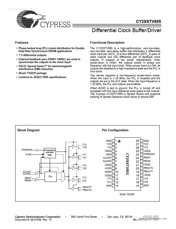
The CY2SSTV855 is a high-performance, very-low-skew, very-low-jitter zero-delay buffer that distributes a differential clock input pair (SSTL_2) to four differential (SSTL_2) pairs of clock outputs and one differential pair of feedback clock outputs. In support of low power requirements, when power-down is HIGH, the outputs switch in phase and frequency with the input clock. When power-down is LOW, all outputs are disabled to a high-impedance state and the PLL is shut down. The device supports a low-frequency power-down mode. When the input is < 20 MHz, the PLL is disabled and the outputs are put in the Hi-Z state. When the input frequency is > 20 MHz, the PLL and outputs are enabled. When AVDD is tied to ground, the PLL is turned off and bypassed with the input reference clock gated to the outputs. The Cypress CY2SSTV855 is Spread Aware and supports tracking of Spread Spectrum clock inputs to reduce EMI
Block Diagram
Pin Configuration
GND YC0 YT0 VDDQ GND CLKINT CLKINC VDDQ AVDD AGND
PLL YT3 YC3 FBOUTT FBOUTC
YT0 YC0 PWRDWN AVDD
Po...
Similar Datasheet