www.DataSheet4U.com
CY29943
2.5V or 3.3V 200-MHz 1:18 Clock Distribution Buffer
Features
• • • • • • • • • • 200-MHz cl...
www.DataSheet4U.com
CY29943
2.5V or 3.3V 200-MHz 1:18 Clock Distribution Buffer
Features
200-MHz clock support 2.5V or 3.3V operation LVPECL clock input LV
CMOS-/LVTTL-compatible inputs 18 clock outputs: drive up to 36 clock lines 200 ps max. output-to-output skew Output Enable control Pin compatible with MPC942P Available in Industrial and Commercial 32-pin LQFP package
Description
The CY29943 is a low-
voltage 200-MHz clock distribution buffer with an LVPECL-compatible input clock. All other control inputs are LV
CMOS-/LVTTL-compatible. The eighteen outputs are 2.5V or 3.3V LV
CMOS- or LVTTL-compatible and can drive 50Ω series or parallel terminated transmission lines. For series terminated transmission line, each output can drive one or two traces giving the device an effective fanout of 1:36. Low output-to-output skews make the CY29943 an ideal clock distribution buffer for nested clock trees in the most demanding of synchronous systems.
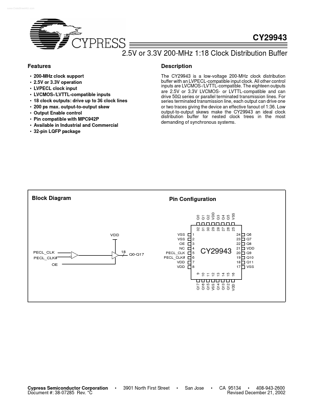
Block Diagram
Pin Configuration
Q0 Q1 Q2 VDD Q3 Q4 Q5 VSS VSS VSS OE NC PECL_CLK PECL_CLK# VDD VDD 1 2 3 4 5 6 7 8 32 31 30 29 28 27 26 25 24 23 22 21 20 19 18 17
VDD
PECL_CLK PECL_CLK# OE
18
Q0-Q17
CY29943
Q6 Q7 Q8 VDD Q9 Q10 Q11 VSS
Cypress Semiconductor Corporation Document #: 38-07285 Rev. *C
3901 North First Street
San Jose
Q17 Q16 Q15 VSS Q14 Q13 Q12 VDD
9 10 11 12 13 14 15 16
CA 95134 408-943-2600 Revised December 21, 2002
CY29943
Pin Description[1]
Pin 5 6 3 9, 10, 11, 13, 14, 15, 18, 19...