2.5 V or 3.3 V, 200 MHz, 1:18 Clock Distribution Buffer
Features
■ 200 MHz clock support ■ LVPECL or LVCMOS/LVTTL clock ...
2.5 V or 3.3 V, 200 MHz, 1:18 Clock Distribution Buffer
Features
■ 200 MHz clock support ■ LVPECL or LV
CMOS/LVTTL clock input ■ LV
CMOS/LVTTL compatible inputs ■ 18 clock outputs: drive up to 36 clock lines ■ 60 ps typical output-to-output skew ■ Dual or single supply operation:
❐ 3.3 V core and 3.3 V outputs ❐ 3.3 V core and 2.5 V outputs ❐ 2.5 V core and 2.5 V outputs ■ Pin compatible with MPC940L, MPC9109 ■ Available in Commercial and Industrial temperature ■ 32-pin TQFP package
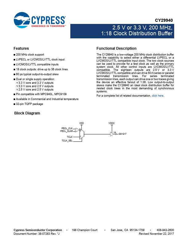
Block Diagram
PECL_CLK PECL_CLK#
TCLK TCLK_SEL
VDD 0 1
CY29940
2.5 V or 3.3 V, 200 MHz, 1:18 Clock Distribution Buffer
Functional Description
The CY29940 is a low-
voltage 200 MHz clock distribution buffer with the capability to select either a differential LVPECL or a LV
CMOS/LVTTL compatible input clock. The two clock sources can be used to provide for a test clock as well as the primary system clock. All other control inputs are LV
CMOS/LVTTL compatible. The eighteen outputs are 2.5...