Global Communications Clock Generator
CY26049-36
FailSafe™ PacketClock™ Global Communications Clock Generator
Features
• Fully integrated phase-locked loop (...
Description
CY26049-36
FailSafe™ PacketClock™ Global Communications Clock Generator
Features
Fully integrated phase-locked loop (PLL) FailSafe output PLL driven by a crystal oscillator that is phase aligned with external reference Output frequencies selectable and/or programmed to standard communication frequencies Low-jitter, high-accuracy outputs Commercial and Industrial operation 3.3V ± 5% operation 16-lead TSSOP When reference is in range, SAFE pin is driven high. When reference is off, DCXO maintains clock outputs. SAFE pin is low. DCXO maintains continuous operation should the input reference clock fail Glitch-free transition simplifies system design Selectable output clock rates include T1/DS1, E1, T3/DS3, E3, and OC-3. Works with commonly available, low-cost 18.432-MHz crystal Zero-ppm error for all output frequencies Performance guaranteed for applications that require an extended temperature range Compatible across industry standard design platforms Industry standard package with 6.4 x 5.0 mm2 footprint and a height profile of just 1.1 mm.
Benefits
Integrated high-performance PLL tailored for telecommunications frequency synthesis eliminates the need for external loop filter components
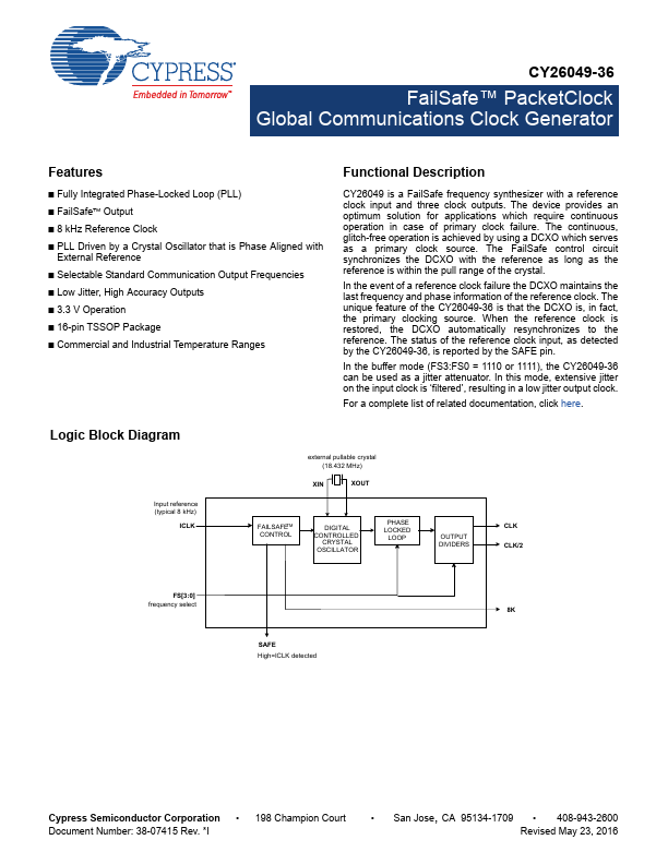
Logic Block Diagram
external pullable crystal (18.432 MHz) XIN Input reference (typical 8 kHz) ICLK
TM FAILSAFE CONTROL
XOUT
DIGITAL CONTROLLED CRYSTAL OSCILLATOR
PHASE LOCKED LOOP
CLK OUTPUT DIVIDERS CLK/2
FS[3:0] frequency select
8K
SAFE High=IC...
Similar Datasheet