Spread Spectrum Clock Generator
CY25561
Spread Spectrum Clock Generator
Features
■ ■ ■ ■
Applications
■ ■ ■ ■
50 to 166 MHz Operating Frequency Range...
Description
CY25561
Spread Spectrum Clock Generator
Features
■ ■ ■ ■
Applications
■ ■ ■ ■
50 to 166 MHz Operating Frequency Range Wide Range of Spread Selections:9 Accepts Clock and Crystal Inputs Low Power Dissipation ❐ 70 mW–Typ at 66 MHz Frequency Spread Disable Function Center Spread Modulation Low Cycle-to-cycle Jitter 8-pin SOIC Package
Desktop, notebook, and tablet PCs VGA controllers LCD panels and monitors Workstations and servers
■ ■ ■ ■
Benefits
■ ■ ■
Peak EMI reduction by 8 to16 dB Fast time to market Cost reduction
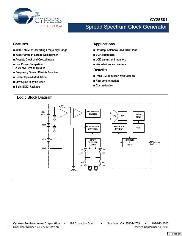
Logic Block Diagram
300 K
Xin/ CLK
1
REFERENCE DIVIDER
PD
CP
Loop Filter
Xout
8
MODULATION CONTROL
FEEDBACK DIVIDER
vco
VDD
2
INPUT DECODER LOGIC
VDD VDD
DIVIDER & MUX
4 SSCLK
VSS
3
20K
20K
20K
VSS
20K
VSS
5 SSCC
6 S1
7 S0
www.DataSheet4U.net
Cypress Semiconductor Corporation Document Number: 38-07242 Rev. *C
198 Champion Court
San Jose, CA 95134-1709 408-943-2600 Revised September 15, 2008
[+] Feedback
CY25561
Pinout
Figure 1. Pin Configuration
XIN/CLK 1 VDD 2 8 XOUT 7 S0
CY25561
VSS 3 SSCLK 4 6 S1 5 SSCC
Table 1. Pin Description Pin Name 1 2 3 4 5 6 Xin/CLK VDD GND SSCLK SSCC S1
Type I P P O I I Positive power supply Power supply ground Modulated clock output
Description Clock or crystal connection input. Refer to Table 2 for input frequency range selection.
Spread spectrum clock control (enable/disable) function. SSCG function is enabled when input is high and disabled when input is low. This pin is pulled hig...
Similar Datasheet