PROCESS
Small Signal Transistor
CP336V
NPN - High Voltage Transistor Chip
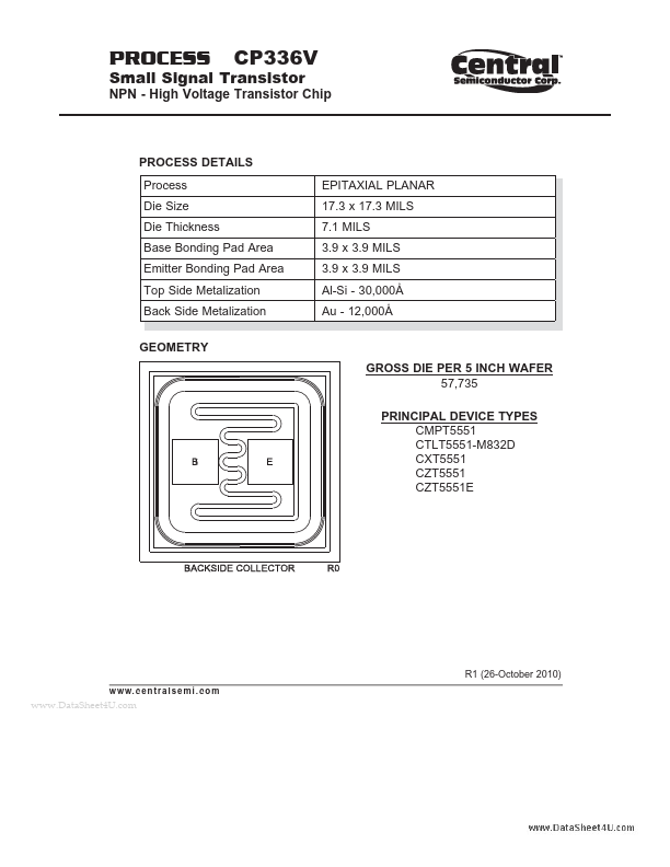
PROCESS DETAILS Process Die Size Die Thick...
PROCESS
Small Signal Transistor
CP336V
NPN - High
Voltage Transistor Chip
PROCESS DETAILS Process Die Size Die Thickness Base Bonding Pad Area Emitter Bonding Pad Area Top Side Metalization Back Side Metalization GEOMETRY GROSS DIE PER 5 INCH WAFER 57,735 PRINCIPAL DEVICE TYPES CMPT5551 CTLT5551-M832D CXT5551 CZT5551 CZT5551E EPITAXIAL PLANAR 17.3 x 17.3 MILS 7.1 MILS 3.9 x 3.9 MILS 3.9 x 3.9 MILS Al-Si - 30,000Å Au - 12,000Å
R1 (26-October 2010)
w w w. c e n t r a l s e m i . c o m
www.DataSheet4U.com
PROCESS
CP336V
Typical Electrical Characteristics
R1 (26-October 2010)
w w w. c e n t r a l s e m i . c o m
www.DataSheet4U.com
...