www.datasheet4u.com
Continental Device India Limited
An ISO/TS 16949, ISO 9001 and ISO 14001 Certified Company
SOT-23 ...
www.datasheet4u.com
Continental Device India Limited
An ISO/TS 16949, ISO 9001 and ISO 14001 Certified Company
SOT-23 Formed SMD Package
CMBT6517
HIGH–
VOLTAGE TRANSISTOR
N–P–N transistor
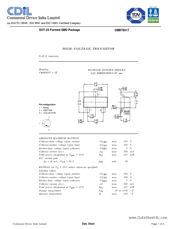
Marking CMBT6517 = 1Z
PACKAGE OUTLINE DETAILS ALL DIMENSIONS IN m m
Pin configuration 1 = BASE 2 = EMITTER 3 = COLLECTOR
3
1
2
ABSOLUTE MAXIMUM RATINGS Collector–base
voltage (open emitter) Collector–emitter
voltage (open base) Emitter–base
voltage (open collector) Collector current (d.c.) Total power dissipation at Tamb = 25°C D.C. current gain –IC = 10 mA; –VCE = 10 V
–V CBO –V CEO –V EBO –IC Ptot hFE
max. max. max. max. max min.
350 350 5 500 225 30
V V V mA mW
RATINGS (at TA = 25°C unless otherwise specified) Limiting values Collector–base
voltage (open emitter) –V CBO Collector–emitter
voltage (open base) –V CEO Emitter–base
voltage (open collector) –V EBO Collector current (d.c.) –IC Ptot Total power dissipation at Tamb = 25°C Storage temperature Tstg Junction temperature Tj
max. 350 max. 350 max. 5 max. 500 max 225 –55 to +150 max. 150
V V V mA mW °C °C
Continental Device India Limited
Data Sheet
Page 1 of 3
www.datasheet4u.com
CMBT6517
THERMAL CHARACTERISTICS Tj = P (Rth j–t + Rth s–a) + Tamb Thermal resistance from junction to ambient
Rth j–a
556
°C/mW
CHARACTERISTICS (at TA = 25°C unless otherwise specified) Collector–emitter breakdown
voltage –IC = 1 mA –V(BR)CEO min. Collector–base breakdown
voltage –IC = 100 µA –V(BR)CBO min. Emitter–base breakdown volt...