CLC402 Low-Gain Op Amp with Fast 14-Bit Settling
June 1999
N
CLC402 Low-Gain Op Amp with Fast 14-Bit Settling
General ...
CLC402 Low-Gain Op Amp with Fast 14-Bit Settling
June 1999
N
CLC402 Low-Gain Op Amp with Fast 14-Bit Settling
General Description Features
s s s s s
0.0025% settling in 25ns (32ns max) 0.5mV input offset
voltage, 3µV/°C drift ±1 to ±8 closed-loop gain range Low power, 150mW 0.01%/0.05° differential gain/phase High-accuracy A/D systems (12-14 bits) High-accuracy D/A converters High-speed communications IF processors Video distribution
Applications
s s s s s
The CLC402 is available in several versions to meet a variety of requirements. A three-letter suffix determines the version: CLC402AJP -40°C to +85°C CLC402AJE -40°C to +85°C CLC402A8B -55°C to +125°C 8-pin plastic DIP 8-pin plastic SOIC 8-pin hermetic CERDIP, MIL-STD-833, Level B dice CLC402ALC -40°C to +85°C CLC402AMC -55°C to +125°C dice qualified to Method 5008, MIL-STD-883, Level B DESC SMD number: 5962-92033
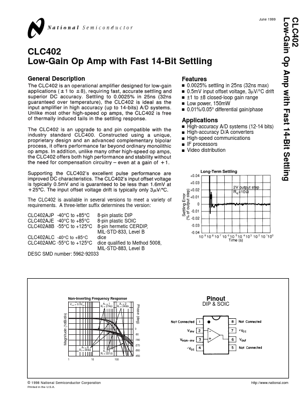
Non-Inverting Frequency Response
Vout = 0.5Vpp Av = 1 Rf = 274Ω Av = 2 Rf = 249Ω
Pinout
DIP & SOIC
Phase (deg)
Magnitude (1dB/div)
0 -90 -180
Av = 8 Rf = 200Ω
-270
Av = 4 Rf = 221Ω
-360 -450 100
1
10
© 1998 National Semiconductor Corporation
Printed in the U.S.A.
http://www.national.com
CLC402 Electrical Characteristics (Av = +2, Vcc = ±5V, RL = 100Ω, Rf = 250Ω; unless specified)
Min/max ratings are based on product characterization and simulation. Individual parameters are tested as noted. Outgoing quality levels are determined from tested parameters.
Absolute Maximum Ratings
Miscellaneous Rati...