CEP61A2/CEB61A2
N-Channel Enhancement Mode Field Effect Transistor FEATURES
20V, 57A, RDS(ON) = 12mΩ @VGS = 4.5V. RDS(ON...
CEP61A2/CEB61A2
N-Channel Enhancement Mode Field Effect Transistor FEATURES
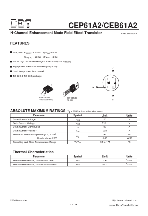
20V, 57A, RDS(ON) = 12mΩ @VGS = 4.5V. RDS(ON) = 20mΩ @VGS = 2.5V. Super high dense cell design for extremely low RDS(ON). High power and current handing capability. Lead free product is acquired. TO-220 & TO-263 package. D PRELIMINARY
D
G
S CEB SERIES TO-263(DD-PAK) G
G D S
CEP SERIES TO-220
S
ABSOLUTE MAXIMUM RATINGS
Parameter Drain-Source
Voltage Gate-Source
Voltage Drain Current-Continuous Drain Current-Pulsed
a
Tc = 25 C unless otherwise noted Symbol Limit VDS VGS ID IDM PD TJ,Tstg 20
Units V V A A W W/ C C
±12
57 228 94 0.63 -55 to 175
Maximum Power Dissipation @ TC = 25 C - Derate above 25 C Operating and Store Temperature Range
Thermal Characteristics
Parameter Thermal Resistance, Junction-to-Case Thermal Resistance, Junction-to-Ambient Symbol RθJC RθJA Limit 1.6 62.5 Units C/W C/W
2004.November 4 - 118
http://www.cetsemi.com
CEP61A2/CEB61A2
Electrical Characteristics
Parameter Off Characteristics Drain-Source Breakdown
Voltage Zero Gate
Voltage Drain Current Gate Body Leakage Current, Forward Gate Body Leakage Current, Reverse On Characteristics b Gate Threshold
Voltage Static Drain-Source On-Resistance Forwand Transconductance Dynamic Characteristics Input Capacitance Output Capacitance Reverse Transfer Capacitance Switching Characteristics c Turn-On Delay Time Turn-On Rise Time Turn-Off Delay Time Turn-On Fall Time Total Gate Charge Gate-Source Charge Gate-Drain Charge Drain-Sour...