CEP10N4/CEB10N4 CEI10N4/CEF10N4
N-Channel Enhancement Mode Field Effect Transistor FEATURES
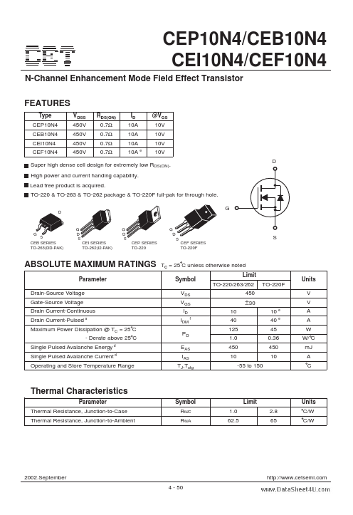
Type CEP10N4 CEB10N4 CEI10N4...
CEP10N4/CEB10N4 CEI10N4/CEF10N4
N-Channel Enhancement Mode Field Effect Transistor FEATURES
Type CEP10N4 CEB10N4 CEI10N4 CEF10N4 VDSS 450V 450V 450V 450V RDS(ON) 0.7Ω 0.7Ω 0.7Ω 0.7Ω ID 10A 10A 10A 10A e @VGS 10V 10V 10V 10V D
Super high dense cell design for extremely low RDS(ON). High power and current handing capability. Lead free product is acquired. TO-220 & TO-263 & TO-262 package & TO-220F full-pak for through hole.
D
G
S CEB SERIES TO-263(DD-PAK)
G
G D S
CEI SERIES TO-262(I2-PAK)
G D S
CEP SERIES TO-220
G
D S
CEF SERIES TO-220F
S
ABSOLUTE MAXIMUM RATINGS
Parameter Drain-Source
Voltage Gate-Source
Voltage Drain Current-Continuous Drain Current-Pulsed
a
Tc = 25 C unless otherwise noted Limit Symbol TO-220/263/262 VDS VGS ID IDM PD EAS IAS TJ,Tstg
f
TO-220F
Units V V
450
±30
10 40 125 1.0 450 10 -55 to 150 10 40 45 0.36 450 10
e e
A A W W/ C mJ A C
Maximum Power Dissipation @ TC = 25 C - Derate above 25 C Single Pulsed Avalanche Energy d Single Pulsed Avalanche Current d Operating and Store Temperature Range
Thermal Characteristics
Parameter Thermal Resistance, Junction-to-Case Thermal Resistance, Junction-to-Ambient Symbol RθJC RθJA 1.0 62.5 Limit 2.8 65 Units C/W C/W
2002.September 4 - 50
http://www.cetsemi.com
CEP10N4/CEB10N4 CEI10N4/CEF10N4
Electrical Characteristics
Parameter Off Characteristics Drain-Source Breakdown
Voltage Zero Gate
Voltage Drain Current Gate Body Leakage Current, Forward Gate Body Leakage Current, Reverse On Characteristics b...