CEN2301
P-Channel Enhancement Mode Field Effect Transistor
FEATURES
-20V, -2.7A, RDS(ON) = 110mΩ @VGS = -4.5V. RDS(ON) ...
CEN2301
P-Channel Enhancement Mode Field Effect Transistor
FEATURES
-20V, -2.7A, RDS(ON) = 110mΩ @VGS = -4.5V. RDS(ON) = 160mΩ @VGS = -2.5V.
High dense cell design for extremely low RDS(ON). Rugged and reliable. Lead-free plating ; RoHS compliant. SOT-23-T package.
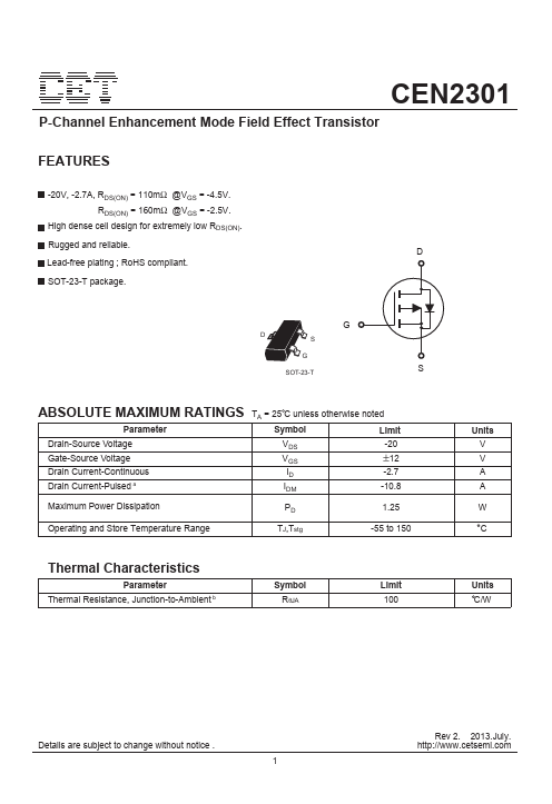
D
DS G
SOT-23-T
G
S
ABSOLUTE MAXIMUM RATINGS TA = 25 C unless otherwise noted
Parameter
Symbol
Limit
Drain-Source
Voltage Gate-Source
Voltage
VDS -20
VGS ±12
Drain Current-Continuous Drain Current-Pulsed a
ID -2.7 IDM -10.8
Maximum Power Dissipation
PD 1.25
Operating and Store Temperature Range
TJ,Tstg
-55 to 150
Thermal Characteristics
Parameter Thermal Resistance, Junction-to-Ambient b
Symbol RθJA
Limit 100
Units V V A A W C
Units C/W
Details are subject to change without notice .
1
Rev 2. 2013.July. http://www.cetsemi.com
CEN2301
Electrical Characteristics TA = 25 C unless otherwise noted
Parameter
Symbol
Test Condition
Min Typ Max Units
Off Characteristics
Drain-Source Breakdown Vol...