CEM4063
P-Channel Enhancement Mode Field Effect Transistor
PRELIMINARY
FEATURES
-40V, -13A, RDS(ON) = 10mΩ @VGS = -10...
CEM4063
P-Channel Enhancement Mode Field Effect Transistor
PRELIMINARY
FEATURES
-40V, -13A, RDS(ON) = 10mΩ @VGS = -10V. RDS(ON) = 14mΩ @VGS = -4.5V.
Super high dense cell design for extremely low RDS(ON). High power and current handing capability. Lead-free plating ; RoHS compliant. Surface mount Package.
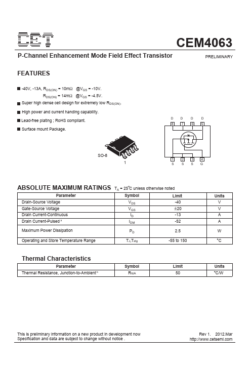
DD D D 8 7 65
SO-8
1
1 234 S SSG
ABSOLUTE MAXIMUM RATINGS TA = 25 C unless otherwise noted
Parameter
Symbol
Limit
Drain-Source
Voltage Gate-Source
Voltage
VDS -40
VGS ±20
Drain Current-Continuous Drain Current-Pulsed a
ID -13 IDM -52
Maximum Power Dissipation
PD 2.5
Operating and Store Temperature Range
TJ,Tstg
-55 to 150
Thermal Characteristics
Parameter Thermal Resistance, Junction-to-Ambient b
Symbol RθJA
Limit 50
Units V V A A W C
Units C/W
This is preliminary information on a new product in development now Specification and data are subject to change without notice .
Rev 1. 2012.Mar http://www.cetsemi.com
CEM4063
Electrical Characteristics TA = 25 C unless otherwise noted
Parameter
Symbol
Test Condition
Off Characteristics
Drain-Source Breakdown
Voltage Zero Gate
Voltage Drain Current Gate Body Leakage Current, Forward Gate Body Leakage Current, Reverse On Characteristics c
BVDSS IDSS IGSSF IGSSR
VGS = 0V, ID = -250µA VDS = -40V, VGS = 0V VGS = 20V, VDS = 0V VGS = -20V, VDS = 0V
Gate Threshold
Voltage Static Drain-Source On-Resistance Dynamic Characteristics d
VGS(th) RDS(on)
VGS = VDS, ID = -250µA VGS = -10V, ID = -6.5A VGS = -4.5V...