CD74HC4016
Data sheet acquired from Harris Semiconductor SCHS199C
February 1998 - Revised August 2004
High-Speed CMOS ...
CD74HC4016
Data sheet acquired from Harris Semiconductor SCHS199C
February 1998 - Revised August 2004
High-Speed
CMOS Logic Quad Bilateral Switch
[ /Title (CD74 HC4016 ) /Subject (HighSpeed
CMOS Logic Quad Bilat-
Features
Description
Wide Analog-Input-
Voltage Range . . . . . . . . . 0V to 10V
Low “ON” Resistance - 45Ω (Typ) . . . . . . . . . . . . . . . . . . . . . . . . . . .VCC = 4.5V - 35Ω (Typ) . . . . . . . . . . . . . . . . . . . . . . . . . . . . VCC = 6V - 30Ω (Typ) . . . . . . . . . . . . . . . . . . . . . . . . . .1fcVCC = 9V
Fast Switching and Propagation Delay Times
Low “OFF” Leakage Current
Built-In “Break-Before-Make” Switching
Suitable for Sample and Hold Applications Wide Operating Temperature Range . . . -55oC to 125oC
HC Types - 2V to 10V Operation - High Noise Immunity: NIL = 30%, NIH = 30% of VCC at VCC = 5V
The CD74HC4016 contains four independent digitally controlled analog switches that use silicon-gate
CMOS technology to achieve operating speeds similar to LSTTL with the low power consumption of standard
CMOS integrated circuits.
Each switch has two input/output terminals (nY, nZ) and an active high enable input (nE). Current through the switch will not cause additional VCC current provided the analog
voltage is maintained between VCC and GND.
Ordering Information
PART NUMBER CD74HC4016E CD74HC4016M CD74HC4016MT CD74HC4016M96 CD74HC4016PW
TEMP. RANGE (oC)
-55 to 125 -55 to 125 -55 to 125 -55 to 125 -55 to 125
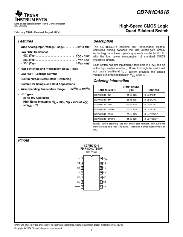
PACKAGE 14 Ld PDI...