CD54HC4015, CD74HC4015
Data sheet acquired from Harris Semiconductor SCHS198C
November 1997 - Revised May 2003
High Sp...
CD54HC4015, CD74HC4015
Data sheet acquired from Harris Semiconductor SCHS198C
November 1997 - Revised May 2003
High Speed
CMOS Logic Dual 4-Stage Static Shift Register
[ /Title (CD74 HC401 5) /Subject (High Speed
CMOS Logic Dual 4-
Features
Description
Maximum Frequency, Typically 60MHz CL = 15pF, VCC = 5V, TA = 25oC
Positive-Edge Clocking
Overriding Reset
Buffered Inputs and Outputs
Fanout (Over Temperature Range)
- Standard Outputs . . . . . . . . . . . . . . . 10 LSTTL Loads - Bus Driver Outputs . . . . . . . . . . . . . 15 LSTTL Loads Wide Operating Temperature Range . . . -55oC to 125oC
Balanced Propagation Delay and Transition Times
Significant Power Reduction Compared to LSTTL Logic ICs
HC Types - 2V to 6V Operation - High Noise Immunity: NIL = 30%, NIH = 30% of VCC at VCC = 5V
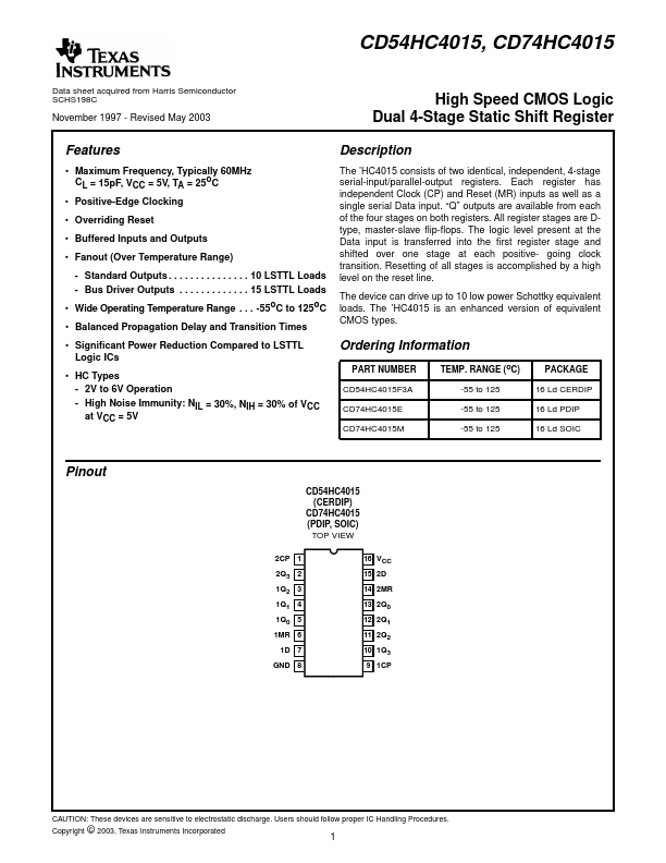
The ’HC4015 consists of two identical, independent, 4-stage serial-input/parallel-output registers. Each register has independent Clock (CP) and Reset (MR) inputs as well as a single serial Data input. “Q” outputs are available from each of the four stages on both registers. All register stages are Dtype, master-slave flip-flops. The logic level present at the Data input is transferred into the first register stage and shifted over one stage at each positive- going clock transition. Resetting of all stages is accomplished by a high level on the reset line.
The device can drive up to 10 low power Schottky equivalent loads. The ’HC4015 is an enhanced version of equivalent
CMOS...