CD54ACT139, CD74ACT139 DUAL 2-LINE TO 4-LINE DECODERS/DEMULTIPLEXERS
D AC Types Feature 1.5-V to 5.5-V Operation
and Ba...
CD54ACT139, CD74ACT139 DUAL 2-LINE TO 4-LINE DECODERS/DEMULTIPLEXERS
D AC Types Feature 1.5-V to 5.5-V Operation
and Balanced Noise Immunity at 30% of the
Supply
Voltage
D Buffered Inputs D Incorporate Two Enable Inputs to Simplify
Cascading and/or Data Reception
D Speed of Bipolar F, AS, and S, With
Significantly Reduced Power Consumption
D Balanced Propagation Delays D ±24-mA Output Drive Current
– Fanout to 15 F Devices
D SCR-Latchup-Resistant
CMOS Process and
Circuit Design
D Exceeds 2-kV ESD Protection Per
MIL-STD-883, Method 3015
SCHS337 – MARCH 2003
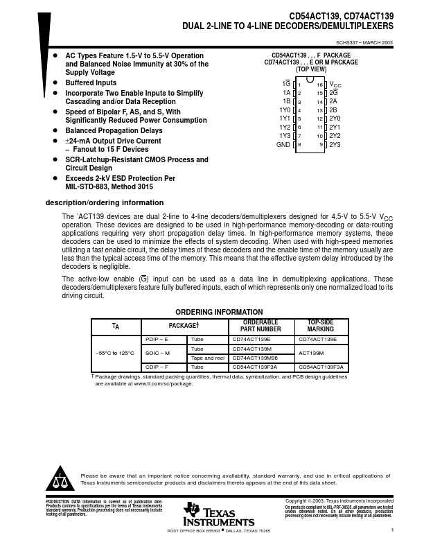
CD54ACT139 . . . F PACKAGE CD74ACT139 . . . E OR M PACKAGE
(TOP VIEW)
1G 1 1A 2 1B 3 1Y0 4 1Y1 5 1Y2 6 1Y3 7 GND 8
16 VCC 15 2G 14 2A 13 2B 12 2Y0 11 2Y1 10 2Y2 9 2Y3
description/ordering information
The ’ACT139 devices are dual 2-line to 4-line decoders/demultiplexers designed for 4.5-V to 5.5-V VCC operation. These devices are designed to be used in high-performance memory-decoding or data-routing applications requiring very short propagation delay times. In high-performance memory systems, these decoders can be used to minimize the effects of system decoding. When used with high-speed memories utilizing a fast enable circuit, the delay times of these decoders and the enable time of the memory usually are less than the typical access time of the memory. This means that the effective system delay introduced by the decoders is negligible.
The active-low enable (G) input can be used as a data line in demultiplexing appl...