CD54AC112, CD74AC112
DUAL J-K NEGATIVE-EDGE-TRIGGERED FLIP-FLOPS WITH CLEAR AND PRESET
SCHS325 – JANUARY 2003
D AC Type...
CD54AC112, CD74AC112
DUAL J-K NEGATIVE-EDGE-TRIGGERED FLIP-FLOPS WITH CLEAR AND PRESET
SCHS325 – JANUARY 2003
D AC Types Feature 1.5-V to 5.5-V Operation
and Balanced Noise Immunity at 30% of the
Supply
Voltage
D Speed of Bipolar F, AS, and S, With
Significantly Reduced Power Consumption
D Balanced Propagation Delays D ±24-mA Output Drive Current
– Fanout to 15 F Devices
D SCR-Latchup-Resistant
CMOS Process and
Circuit Design
D Exceeds 2-kV ESD Protection Per
MIL-STD-883, Method 3015
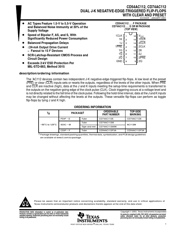
CD54AC112 . . . F PACKAGE CD74AC112 . . . E OR M PACKAGE
(TOP VIEW)
1CLK 1 1K 2 1J 3
1PRE 4 1Q 5 1Q 6 2Q 7
GND 8
16 VCC 15 1CLR 14 2CLR 13 2CLK 12 2K 11 2J 10 2PRE 9 2Q
description/ordering information
The ’AC112 devices contain two independent J-K negative-edge-triggered flip-flops. A low level at the preset (PRE) or clear (CLR) inputs sets or resets the outputs, regardless of the levels of the other inputs. When PRE and CLR are inactive (high), data at the J and K inputs meeting the setup-time requirements is transferred to the outputs on the negative-going edge of the clock pulse (CLK). Clock triggering occurs at a
voltage level and is not directly related to the fall time of the clock pulse. Following the hold-time interval, data at the J and K inputs may be changed without affecting the levels at the outputs. These versatile flip-flops can perform as toggle flip-flops by tying J and K high.
ORDERING INFORMATION
TA
PACKAGE†
ORDERABLE PART NUMBER
TOP-SIDE MARKING
PDIP – E
Tube
CD7...