CD4099BM CD4099BC 8-Bit Addressable Latch
February 1988
CD4099BM CD4099BC 8-Bit Addressable Latch
General Description
...
CD4099BM CD4099BC 8-Bit Addressable Latch
February 1988
CD4099BM CD4099BC 8-Bit Addressable Latch
General Description
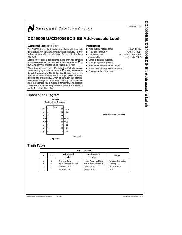
The CD4099B is an 8-bit addressable latch with three address inputs (A0–A2) an active low enable input (E) active high clear input (CL) a data input (D) and eight outputs (Q0 – Q7) Data is entered into a particular bit in the latch when that bit is addressed by the address inputs and the enable (E) is low Data entry is inhibited when enable (E) is high When clear (CL) and enable (E) are high all outputs are low When clear (CL) is high and enable (E) is low the channel demultiplexing occurs The bit that is addressed has an active output which follows the data input while all unaddressed bits are held low When operating in the addressable latch mode (E e CL e low) changing more than one bit of the address could impose a transient wrong address Therefore this should only be done while in the memory mode (E e high CL e low)
Features
Y Y Y
Y Y Y Y Y
Wide supply
voltage range 3 0V to 15V High noise immunity 0 45 VDD (typ ) Low power TTL fan out of 2 driving 74L compatibility or 1 driving 74LS Serial to parallel capability Storage register capability Random (addressable) data entry Active high demultiplexing capability Common active high clear
Connection Diagram
CD4099B Dual-In-Line Package
Order Number CD4099B
TL F 5984 – 1
Top View
Truth Table
Mode Selection E L H L H CL L L H H Addressed Latch Follows Data Holds Previous Data Follows Data Reset to ‘‘0’’ ...