CD4049UBMS
CMOS Hex Buffer/Converter
The CD4049UBMS is an inverting hex buffer and features logic level conversion usin...
CD4049UBMS
CMOS Hex Buffer/Converter
The CD4049UBMS is an inverting hex buffer and features logic level conversion using only one supply (
voltage (VCC). The input signal high level (VIH) can exceed the VCC supply
voltage when this device is used for logic level conversions. This device is intended for use as
CMOS to DTL/TTL converters and can drive directly two DTL/TTL loads. (VCC = 5V, VOL 0.4V, and IOL 3.3mA.
The CD4049UBMS is designated as replacement for CD4009UB. Because the CD4049UBMS requires only one power supply, it is preferred over the CD4009UB and CD4010B and should be used in place of the CD4009UB in all inverter, current driver, or logic level conversion applications. In these applications the CD4049UBMS is pin compatible with the CD4009UB, and can be substituted for this device in existing as well as in new designs. Terminal No. 16 is not connected internally on the CD4049UBMS, therefore, connection to this terminal is of no consequence to circuit operation. For applications not requiring high sink current or
voltage conversion, the CD4069UB Hex Inverter is recommended.
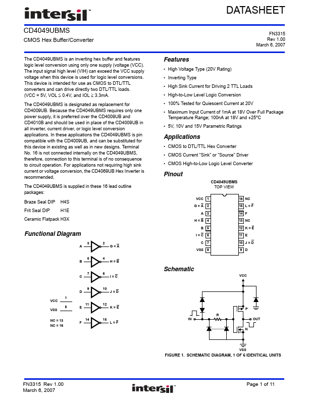
The CD4049UBMS is supplied in these 16 lead outline packages:
Braze Seal DIP H4S
Frit Seal DIP H1E
Ceramic Flatpack H3X
Functional Diagram
3 A
5 B
7 C
1 VCC
8 VSS
NC = 13 NC = 16
9 D
11 E
14 F
2 G=A
4 H=B
6 I=C
10 J=D
12 K=E
15 L=F
DATASHEET
FN3315 Rev 1.00 March 6, 2007
Features
High
Voltage Type (20V Rating) Inverting Type High Sink Current for Driving 2 TTL Loads High-to...