CD4030BMS
December 1992
CMOS Quad Exclusive-OR Gate
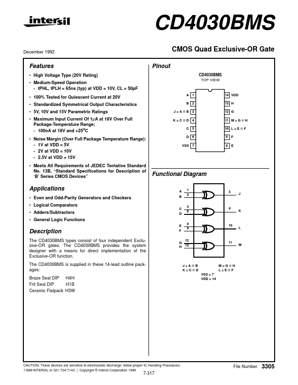
Pinout
CD4030BMS TOP VIEW
Features
• High Voltage Type (20V Rating...
CD4030BMS
December 1992
CMOS Quad Exclusive-OR Gate
Pinout
CD4030BMS TOP VIEW
Features
High
Voltage Type (20V Rating) Medium-Speed Operation - tPHL, tPLH = 65ns (typ) at VDD = 10V, CL = 50pF 100% Tested for Quiescent Current at 20V Standardized Symmetrical Output Characteristics 5V, 10V and 15V Parametric Ratings Maximum Input Current Of 1µA at 18V Over Full Package-Temperature Range; - 100nA at 18V and +25oC Noise Margin (Over Full Package Temperature Range): - 1V at VDD = 5V - 2V at VDD = 10V - 2.5V at VDD = 15V Meets All Requirements of JEDEC Tentative Standard No. 13B, “Standard Specifications for Description of ‘B’ Series
CMOS Devices”
A 1 B 2 J=A⊕B 3 K=C⊕D 4 C 5 D 6 VSS 7
14 VDD 13 H 12 G 11 M = G ⊕ H 10 L = E ⊕ F 9 F 8 E
Functional Diagram
A B 1 2 3
Applications
Even and Odd-Parity Generators and Checkers Logical Comparators Adders/Subtractors General Logic Functions
J
C D
5 6
4
K
Description
The CD4030BMS types consist of four independent Exclusive-OR gates. The CD4030BMS provides the system designer with a means for direct implementation of the Exclusive-OR function. The CD4030BMS is supplied in these 14-lead outline packages: Braze Seal DIP H4H Frit Seal DIP H1B Ceramic Flatpack H3W
E F
8 9
10
L
12 G H 13
11
M
J=A⊕B K=C⊕D VSS = 7 VDD = 14
M=G⊕H L=E⊕F
CAUTION: These devices are sensitive to electrostatic discharge; follow proper IC Handling Procedures. 1-888-INTERSIL or 321-724-7143 | Copyright © Intersil Corporation 1999
...