SIPMOS® Small-Signal Transistor
BSS 135
q q q q q q q
VDS 600 V ID 0.080 A RDS(on) 60 Ω
N channel Depletion mode High...
SIPMOS® Small-Signal Transistor
BSS 135
q q q q q q q
VDS 600 V ID 0.080 A RDS(on) 60 Ω
N channel Depletion mode High dynamic resistance Available grouped in VGS(th)
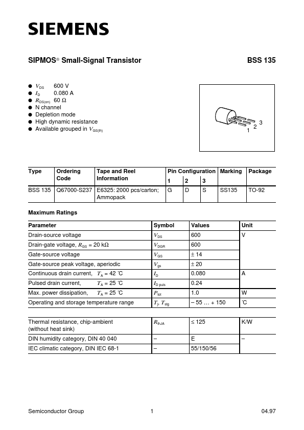
1
2
3
Type
Ordering Code
Tape and Reel Information
Pin Configuration Marking 1 G 2 D 3 S SS135
Package TO-92
BSS 135 Q67000-S237 E6325: 2000 pcs/carton; Ammopack Maximum Ratings Parameter Drain-source
voltage Drain-gate
voltage, RGS = 20 kΩ Gate-source
voltage Gate-source peak
voltage, aperiodic Continuous drain current, TA = 42 ˚C Pulsed drain current, Max. power dissipation,
Symbol
Values 600 600 ± 14 ± 20 0.080 0.24 1.0 – 55 … + 150 ≤ 125 E 55/150/56
Unit V
VDS VDGR VGS Vgs ID ID puls Ptot Tj, Tstg RthJA
– –
A W ˚C K/W –
TA = 25 ˚C TA = 25 ˚C
Operating and storage temperature range Thermal resistance, chip-ambient (without heat sink) DIN humidity category, DIN 40 040 IEC climatic category, DIN IEC 68-1
Semiconductor Group
1
04.97
BSS 135
Electrical Characteristics at Tj = 25 ˚C, unless otherwise specified. Parameter Symbol min. Static Characteristics Drain-source breakdown
voltage VGS = − 3 V, ID = 0.25 mA Gate threshold
voltage VDS = 3 V, ID = 1 mA Drain-source cutoff current VDS = 600 V, VGS = − 3 V Tj = 25 ˚C Tj = 125 ˚C Gate-source leakage current VGS = 20 V, VDS = 0 Drain-source on-resistance VGS = 0 V, ID = 0.01 A Dynamic Characteristics Forward transconductance VDS ≥ 2 × ID × RDS(on)max, ID = 0.01 A Input capacitance VGS = − 3 V, VDS = 25 V, f = 1 MHz Output capacitance VGS = − 3...