w
at • N-Channel .D w • Enhancement mode w • Logic Level
Features • dv/dt rated
SIPMOS ® Small-Signal-Transistor
Produ...
w
at N-Channel .D w Enhancement mode w Logic Level
Features dv/dt rated
SIPMOS ® Small-Signal-Transistor
Product Summary Drain source
voltage Continuous drain current
h S a
ee
U 4 t
m o .c
Preliminary data
BSP308
VDS ID
4
30 0.05 4.7
V Ω A
Drain-Source on-state resistance RDS(on)
Type BSP308
Package SOT-223
Ordering Code Q67000-S4011
Maximum Ratings,at T j = 25 °C, unless otherwise specified Parameter Symbol Continuous drain current
T A = 25 °C T A = 70 °C
Pulsed drain current
T A = 25 °C
Reverse diode dv/dt
I S = 4.7 A, V DS = 20 V, di/dt = 200 A/µs, T jmax = 150 °C
Gate source
voltage Power dissipation
w
w
w
t a .D
S a
e h
ID
U 4 t e
.c
G
m o
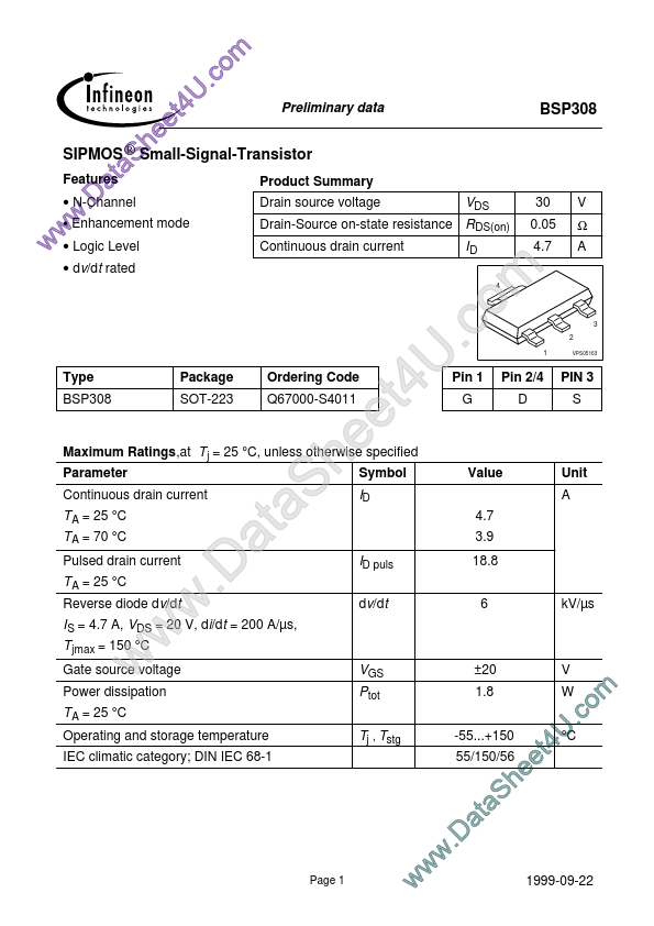
2 1
3
VPS05163
Pin 1
Pin 2/4 D
PIN 3 S
Value 4.7 3.9
Unit A
ID puls
dv/dt
18.8 6 kV/µs
VGS Ptot Tj , Tstg
±20 1.8 -55...+150 55/150/56
V
T A = 25 °C
Operating and storage temperature IEC climatic category; DIN IEC 68-1
Page 1
w
w
w
.D
a
S a t
e e h
m o c . °C U 4 t
W
1999-09-22
Preliminary data
Thermal Characteristics Parameter Characteristics Thermal resistance, junction - soldering point SMD version, device on PCB: @ min. footprint @ 6 cm 2 cooling area 1) Symbol min. Values typ. -
BSP308
Unit max. 25 110 70 K/W K/W
RthJS RthJA
-
Electrical Characteristics , at T j = 25 °C, unless otherwise specified Parameter Static Characteristics Drain- source breakdown
voltage Symbol min. Values typ. 1.6 max. 2 µA 0.1 10 10 0.05 0.03 1 100 100 0.075 0.05 nA Ω Ω V Unit
V(BR)DSS VGS(t...