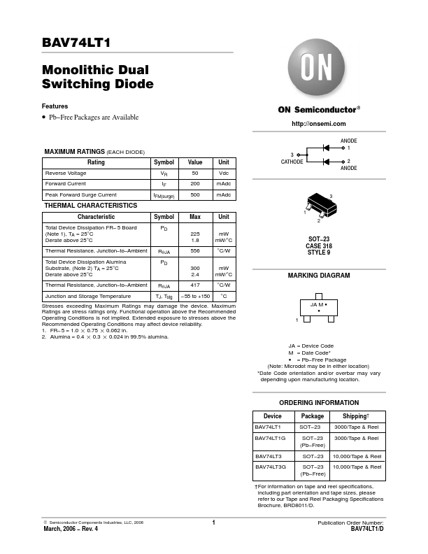
www.DataSheet4U.com
BAV74LT1 Monolithic Dual Switching Diode
Features
• Pb−Free Packages are Available
http://onsemi....
www.DataSheet4U.com
BAV74LT1 Monolithic Dual Switching Diode
Features
Pb−Free Packages are Available
http://onsemi.com
ANODE 1 2 ANODE
MAXIMUM RATINGS (EACH DIODE)
Rating Reverse
Voltage Forward Current Peak Forward Surge Current Symbol VR IF IFM(surge) Value 50 200 500 Unit Vdc mAdc mAdc
3 CATHODE
3 1 2
THERMAL CHARACTERISTICS
Characteristic Total Device Dissipation FR− 5 Board (Note 1), TA = 25°C Derate above 25°C Thermal Resistance, Junction−to−Ambient Total Device Dissipation Alumina Substrate, (Note 2) TA = 25°C Derate above 25°C Thermal Resistance, Junction−to−Ambient Junction and Storage Temperature Symbol PD 225 1.8 RqJA PD 300 2.4 RqJA TJ, Tstg 417 −55 to +150 mW mW/°C °C/W °C JA M G G 1 556 mW mW/°C °C/W SOT−23 CASE 318 STYLE 9 Max Unit
MARKING DIAGRAM
Stresses exceeding Maximum Ratings may damage the device. Maximum Ratings are stress ratings only. Functional operation above the Recommended Operating Conditions is not implied. Extended exposure to stresses above the Recommended Operating Conditions may affect device reliability. 1. FR−5 = 1.0 0.75 0.062 in. 2. Alumina = 0.4 0.3 0.024 in 99.5% alumina.
JA = Device Code M = Date Code* G = Pb−Free Package (Note: Microdot may be in either location) *Date Code orientation and/or overbar may vary depending upon manufacturing location.
ORDERING INFORMATION
Device BAV74LT1 BAV74LT1G BAV74LT3 BAV74LT3G Package SOT−23 SOT−23 (Pb−Free) SOT−23 SOT−23 (Pb−Free) Shipping† 3000/Tape & Reel 3000/Tape & Reel 10...