www.DataSheet4U.com
BAV70TT1
Preferred Device
Dual Switching Diode
Features
• Pb−Free Package May be Available.* The ...
www.DataSheet4U.com
BAV70TT1
Preferred Device
Dual Switching Diode
Features
Pb−Free Package May be Available.* The G−Suffix Denotes a
Pb−Free Lead Finish
http://onsemi.com
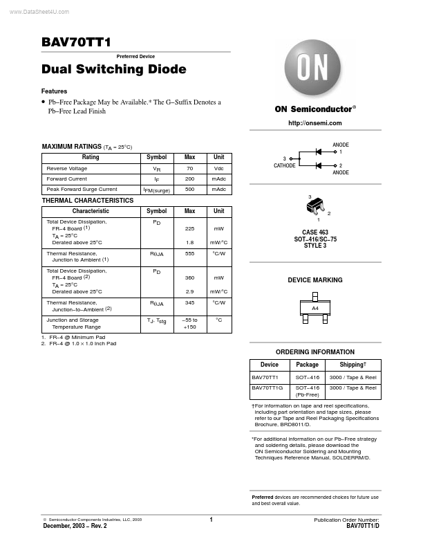
ANODE 1 2 ANODE
MAXIMUM RATINGS (TA = 25°C)
Rating Reverse
Voltage Forward Current Peak Forward Surge Current Symbol VR IF IFM(surge) Max 70 200 500 Unit Vdc mAdc mAdc 3 Symbol PD 225 1.8 RqJA PD 360 2.9 RqJA TJ, Tstg 345 −55 to +150 mW mW/°C °C/W A4 °C 555 mW mW/°C °C/W Max Unit 1 2 3 CATHODE
THERMAL CHARACTERISTICS
Characteristic Total Device Dissipation, FR−4 Board (1) TA = 25°C Derated above 25°C Thermal Resistance, Junction to Ambient (1) Total Device Dissipation, FR−4 Board (2) TA = 25°C Derated above 25°C Thermal Resistance, Junction−to−Ambient (2) Junction and Storage Temperature Range 1. FR−4 @ Minimum Pad 2. FR−4 @ 1.0 × 1.0 Inch Pad
CASE 463 SOT−416/SC−75 STYLE 3
DEVICE MARKING
ORDERING INFORMATION
Device BAV70TT1 BAV70TT1G Package SOT−416 SOT−416 (Pb-Free) Shipping† 3000 / Tape & Reel 3000 / Tape & Reel
†For information on tape and reel specifications, including part orientation and tape sizes, please refer to our Tape and Reel Packaging Specifications Brochure, BRD8011/D. *For additional information on our Pb−Free strategy and soldering details, please download the ON Semiconductor Soldering and Mounting Techniques Reference Manual, SOLDERRM/D.
Preferred devices are recommended choices for future use and best overall value.
© Semiconductor Components Industries, LLC, 2003
1
Decemb...