www.DataSheet4U.com
BAS16DXV6T1, BAS16DXV6T5
Preferred Device
Dual Switching Diode
Features
• Pb−Free Packages are Av...
www.DataSheet4U.com
BAS16DXV6T1, BAS16DXV6T5
Preferred Device
Dual Switching Diode
Features
Pb−Free Packages are Available
MAXIMUM RATINGS (TA = 25°C)
Rating Continuous Reverse
Voltage Recurrent Peak Forward Current Peak Forward Surge Current Pulse Width = 10 ms Symbol VR IF IFM(surge) Max 75 200 500 Unit V mA mA
http://onsemi.com
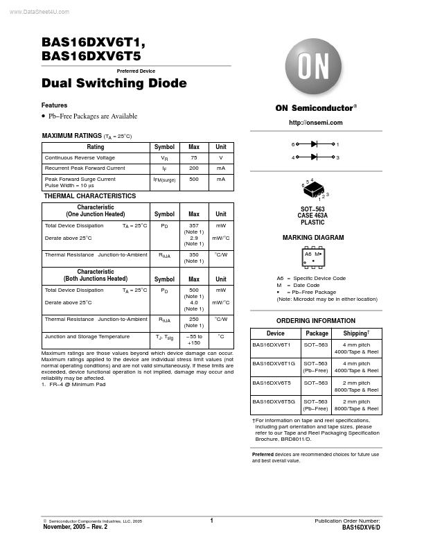
6 4
1 3
6
54 2 3
THERMAL CHARACTERISTICS
Characteristic (One Junction Heated) Total Device Dissipation Derate above 25°C Thermal Resistance Junction-to-Ambient Characteristic (Both Junctions Heated) Total Device Dissipation Derate above 25°C Thermal Resistance Junction-to-Ambient Junction and Storage Temperature RqJA TJ, Tstg TA = 25°C RqJA TA = 25°C Symbol PD Max 357 (Note 1) 2.9 (Note 1) 350 (Note 1) Max 500 (Note 1) 4.0 (Note 1) 250 (Note 1) −55 to +150 Unit mW mW/°C °C/W
1
SOT−563 CASE 463A PLASTIC
MARKING DIAGRAM
A6 MG G A6 = Specific Device Code M = Date Code G = Pb−Free Package (Note: Microdot may be in either location)
Symbol PD
Unit mW mW/°C °C/W °C
ORDERING INFORMATION
Device BAS16DXV6T1 BAS16DXV6T1G BAS16DXV6T5 BAS16DXV6T5G Package SOT−563 SOT−563 (Pb−Free) SOT−563 SOT−563 (Pb−Free) Shipping† 4 mm pitch 4000/Tape & Reel 4 mm pitch 4000/Tape & Reel 2 mm pitch 8000/Tape & Reel 2 mm pitch 8000/Tape & Reel
Maximum ratings are those values beyond which device damage can occur. Maximum ratings applied to the device are individual stress limit values (not normal operating conditions) and are not valid simultaneously. If these l...