www.DataSheet4U.com
Features
• • • • • • • •
User-controlled Power-down Pin High-speed Equivalent of ATF20V8B Pin-contr...
www.DataSheet4U.com
Features
User-controlled Power-down Pin High-speed Equivalent of ATF20V8B Pin-controlled Zero Standby Power (10 µA Typical) Option Industry-standard Architecture – Emulates Many 24-pin PALs® – Low-cost Easy-to-use Software Tools High-speed Electrically-erasable Programmable Logic Devices – 5 ns Maximum Pin-to-pin Delay
CMOS and TTL Compatible Inputs and Outputs – Latch Feature Hold Outputs to Previous Logic States Advanced Flash Technology – Reprogrammable – 100% Tested High-reliability
CMOS Process – 20 Year Data Retention – 100 Erase/Write Cycles – 2,000V ESD Protection – 200 mA Latchup Immunity Commercial, and Industrial Temperature Ranges Dual-in-line and Surface Mount Packages in Standard Pinouts PCI-Compliant
Highperformance EE PLD ATF20V8C ATF20V8CQ Advance Information
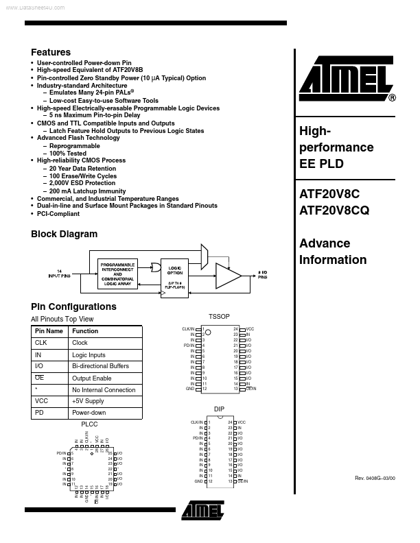
Block Diagram
Pin Configurations
All Pinouts Top View
Pin Name CLK IN I/O OE * VCC PD Function Clock Logic Inputs Bi-directional Buffers Output Enable No Internal Connection +5V Supply Power-down PLCC
IN IN CLK/IN * VCC IN I/O
TSSOP
CLK/IN IN IN PD/ IN IN IN IN IN IN IN IN GND 1 2 3 4 5 6 7 8 9 10 11 12 24 23 22 21 20 19 18 17 16 15 14 13 VCC IN I/O I/O I/O I/O I/O I/O I/O I/O IN OE/IN
DIP
CLK/IN IN IN PD/IN IN IN IN IN IN IN IN GND 1 2 3 4 5 6 7 8 9 10 11 12 24 23 22 21 20 19 18 17 16 15 14 13 VCC IN I/O I/O I/O I/O I/O I/O I/O I/O IN OE/IN
4 3 2 1 28 27 26
IN IN GND * OE/IN IN I/O
12 13 14 15 16 17 18
PD/IN IN IN * IN IN IN
5 6 7 8 9 10 11
25 24 23...