Features
• Fast Read Access Time - 120 ns • Word-wide or Byte-wide Configurable • Dual Voltage Range Operation • • •
– U...
Features
Fast Read Access Time - 120 ns Word-wide or Byte-wide Configurable Dual
Voltage Range Operation
– Unregulated Battery Power Supply Range, 2.7V to 3.6V or Standard 5V ± 10% Supply Range 4-Megabit Flash and Mask ROM Compatable Low Power
CMOS Operation – 20 µA Maximum Standby – 10 mA Max. Active at 5 MHz for VCC = 3.6V JEDEC Standard Packages – 44-Lead PLCC – 44-Lead SOIC (SOP) – 48-Lead TSOP (12 mm x 20 mm) High Reliability
CMOS Technology – 2,000 ESD Protection – 200 mA Latchup Immunity Rapid™ Programming Algorithm - 50 µs/word (typical)
CMOS and TTL Compatible Inputs and Outputs – JEDEC Standard for LVTTL and LVBO Integrated Product Identification Code Commercial and Industrial Temperature Ranges
Description
The AT27BV400 is a high performance low-power, low-
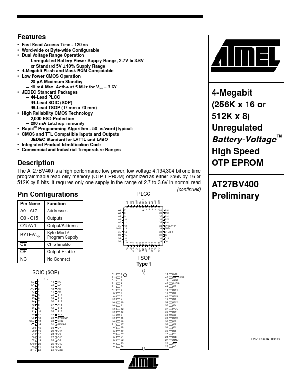
voltage 4,194,304-bit one time programmable read only memory (OTP EPROM) organized as either 256K by 16 or 512K by 8 bits. It requires only one supply in the range of 2.7 to 3.6V in normal read (continued) PLCC Pin Configurations
Pin Name A0 - A17 O0 - O15 O15/A-1 BYTE/VPP CE OE NC Function Addresses Outputs Output/Address Byte Mode/ Program Supply Chip Enable Output Enable No Connect
A4 A3 A2 A1 A0 CE GND OE O0 O8 O1 7 8 9 10 11 12 13 14 15 16 17 6 5 4 3 2 1 44 43 42 41 40 A5 A6 A7 A17 NC GND NC A8 A9 A10 A11 39 38 37 36 35 34 33 32 31 30 29 A12 A13 A14 A15 A16 BYTE/VPP GND O15/A-1 07 O14 O6
4-Megabit (256K x 16 or 512K x 8) Unregulated Battery-
Voltage™ High Speed OTP EPROM AT27BV400 Pre...