June 2005 rev 0.3 2.5V or 3.3V, 200-MHz, 12-Output Zero Delay Buffer
Features
Output frequency r...
June 2005 rev 0.3 2.5V or 3.3V, 200-MHz, 12-Output Zero Delay Buffer
Features
Output frequency range: 8.3MHz to 125MHz Input frequency range: 4.2MHz to 62.5MHz 2.5V or 3.3V operation Split 2.5V/3.3V outputs 14 Clock outputs: Drive up to 28 clock lines 2 LV
CMOS reference clock inputs 150 pS max output-output skew PLL bypass mode ‘SpreadTrak’ Output enable/disable Pin compatible with MPC9774 and CY29774AI. Industrial temperature range: –40°C to +85°C 52Pin 1.0mm TQFP package RoHS Compliance
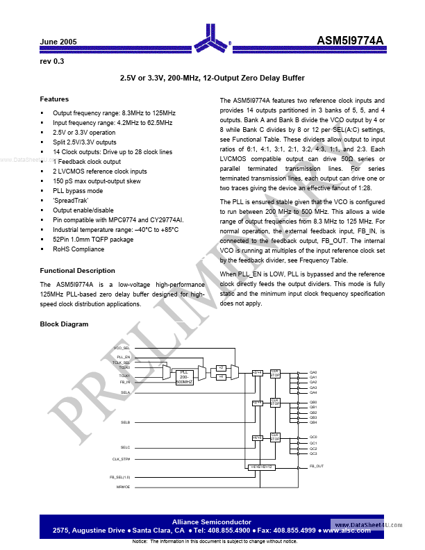
ASM5I9774A
The ASM5I9774A features two reference clock inputs and provides 14 outputs partitioned in 3 banks of 5, 5, and 4 outputs. Bank A and Bank B divide the VCO output by 4 or 8 while Bank C divides by 8 or 12 per SEL(A:C) settings, see Functional Table. These dividers allow output to input ratios of 6:1, 4:1, 3:1, 2:1, 3:2, 4:3, 1:1, and 2:3. Each LV
CMOS compatible output can drive 50Ω series or parallel terminated transmission lines. For series terminated transmission lines, each output can drive one or two traces giving the device an effective fanout of 1:28. The PLL is ensured stable given that the VCO is configured to run between 200 MHz to 500 MHz. This allows a wide range of output frequencies from 8.3 MHz to 125 MHz. For normal operation, the external feedback input, FB_IN, is connected to the feedback output, FB_OUT. The internal VCO is running at multiples of the input reference clock set by the feedback divider, see Frequency Table.
www.DataSheet4U....