| Part Number | ASM5I9350 |
| Manufacturer | Alliance Semiconductor |
| Description | 3.3V 1:10 LVCMOS PLL Clock Generator |
| Published | May 9, 2008 |
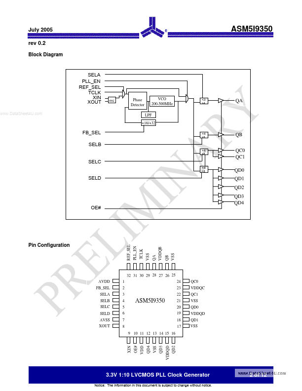
| Detailed Description | July 2005 rev 0.2 3.3V 1:10 LVCMOS PLL Clock Generator Features Output frequency range: 25 MHz to 200 MHz Input fr... |
| Datasheet |
|