July 2005
www.DataSheet4U.com rev 1.0
ASM3P623S00A/B/C/D/E/F
Zero Cycle Slip Peak EMI reduction IC
General Features
...
July 2005
www.DataSheet4U.com rev 1.0
ASM3P623S00A/B/C/D/E/F
Zero Cycle Slip Peak EMI reduction IC
General Features
Input frequency range: 20MHz - 50MHz. Zero input - output propagation delay. Low-skew outputs. Output-output skew less than 250pS. Device-device skew less than 700pS.
All parts have on-chip PLLs that lock to an input clock on the CLKIN pin. The PLL feedback is on-chip and is obtained from the CLKOUT pad, internal to the device. Multiple ASM3P623S00D/E/F devices can accept the same input clock and distribute it. In this case, the skew between the outputs of the two devices is guaranteed to be less than 700pS. All outputs have less than 200pS of cycle-to-cycle jitter. The input and output propagation delay is guaranteed to be less than 250pS, and the output-to-output skew is guaranteed to be less than 250pS. Please refer “Differential Cycle Slips and Spread Spectrum Control Table” for deviations and differential Cycle Slips for ASM3P623S00A/B/C and the ASM3P623S00D/E/F devices
Less than 200pS cycle-to-cycle jitter is compatible with Pentium® based systems. Available in 16pin, 150mil SOIC, 4.4mm TSSOP (ASM3P623S00D/E/F), and in 8pin, 150 mil SOIC, 4.4mm TSSOP Packages (ASM3P623S00A/B/C).
3.3V operation Advanced 0.35µ
CMOS technology. The First True Drop-in Solution.
Functional Description
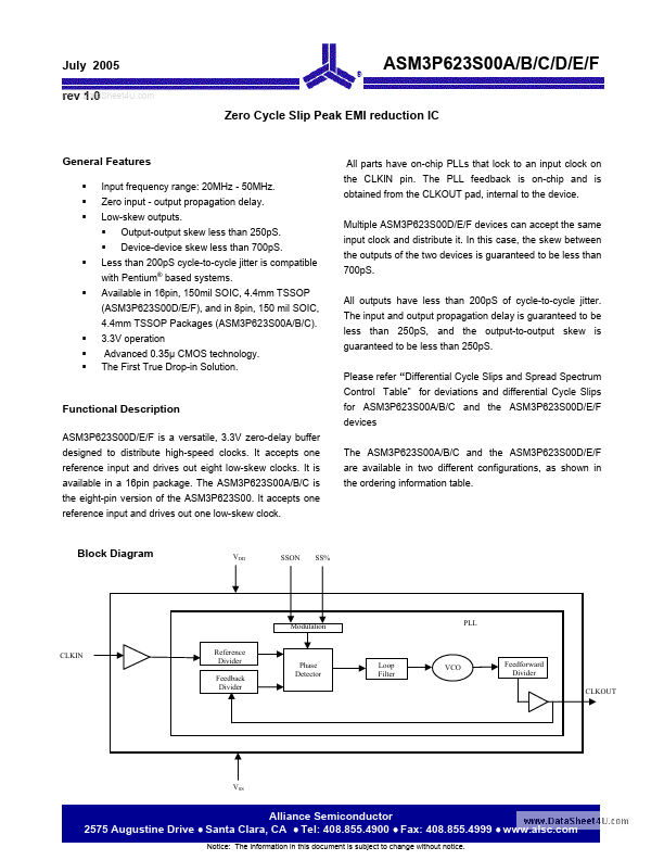
ASM3P623S00D/E/F is a versatile, 3.3V zero-delay buffer designed to distribute high-speed clocks. It accepts one reference input and drives out eight lo...