February 2006
®
AS7C4098A
5.0 V 256 K × 16 CMOS SRAM Features
• Pin compatible with AS7C4098 • Industrial and commerci...
February 2006
®
AS7C4098A
5.0 V 256 K × 16
CMOS SRAM Features
Pin compatible with AS7C4098 Industrial and commercial temperature Organization: 262,144 words × 16 bits Center power and ground pins High speed
- 10/12/15/20 ns address access time - 5/6 ns output enable access time
Easy memory expansion with CE, OE inputs TTL- and
CMOS-compatible, three-state I/O 44-pin JEDEC standard packages ESD protection ≥ 2000 volts Latch-up current ≥ 200 mA
- 400-mil SOJ - TSOP 2
Low power consumption: ACTIVE
- 990mW/max @ 10 ns
Low power consumption: STANDBY
- 55mW/max
CMOS
Individual byte read/write controls
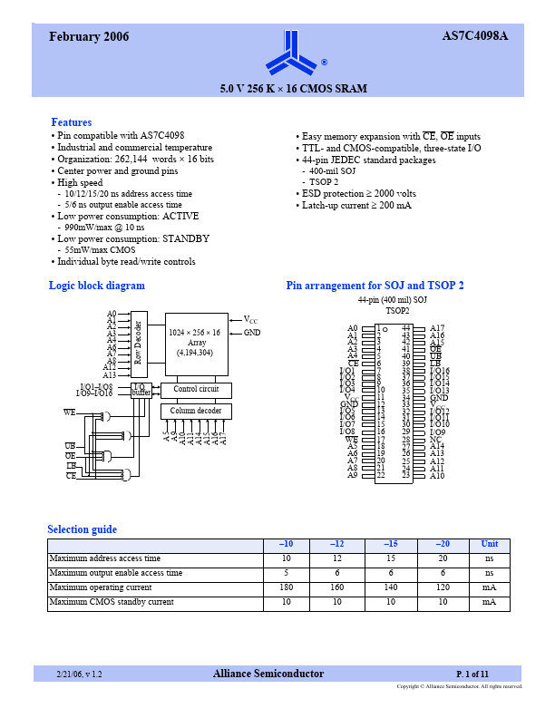
Logic block diagram
A0 A1 A2 A3 A4 A6 A7 A8 A12 A13 I/O1–I/O8 I/O9–I/O16 WE VCC 1024 × 256 × 16 Array (4,194,304) GND
Pin arrangement for SOJ and TSOP 2
44-pin (400 mil) SOJ TSOP2
A0 A1 A2 A3 A4 CE I/O1 I/O2 I/O3 I/O4 VCC GND I/O5 I/O6 I/O7 I/O8 WE A5 A6 A7 A8 A9 1 2 3 4 5 6 7 8 9 10 11 12 13 14 15 16 17 18 19 20 21 22 44 43 42 41 40 39 38 37 36 35 34 33 32 31 30 29 28 27 26 25 24 23 A17 A16 A15 OE UB LB I/O16 I/O15 I/O14 I/O13 GND VCC I/O12 I/O11 I/O10 I/O9 NC A14 A13 A12 A11 A10
I/O buffer
Row Decoder
Control circuit Column decoder
A5 A9 A10 A11 A14 A15 A16 A17
UB OE LB CE
Selection guide
–10 Maximum address access time Maximum output enable access time Maximum operating current Maximum
CMOS standby current 10 5 180 10 –12 12 6 160 10 –15 15 6 140 10 –20 20 6 120 10 Unit ns ns mA mA
2/21/06, v 1.2
Alliance Semiconductor
P. 1 of 11
Copyright ...