March 2002
®
AS7C4098 AS7C34098
5V/3.3V 256K × 16 CMOS SRAM
Features
• AS7C4098 (5V version) • AS7C34098 (3.3V version...
March 2002
®
AS7C4098 AS7C34098
5V/3.3V 256K × 16
CMOS SRAM
Features
AS7C4098 (5V version) AS7C34098 (3.3V version) Industrial and commercial temperature Organization: 262,144 words × 16 bits Center power and ground pins High speed
- 10/12/15/20 ns address access time - 5/6/7/8 ns output enable access time
Low power consumption: STANDBY
- 110 mW (AS7C4098)/max
CMOS - 72 mW (AS7C34098)/max
CMOS
Individual byte read/write controls Easy memory expansion with CE, OE inputs TTL- and
CMOS-compatible, three-state I/O 44-pin JEDEC standard packages
- 400-mil SOJ - TSOP 2 - 48-ball FBGA 7 x 11 mm
Low power consumption: ACTIVE
- 1375 mW (AS7C4098)/max @ 12 ns - 468 mW (AS7C34098)/max @ 12 ns
ESD protection ≥ 2000 volts Latch-up current ≥ 200 mA
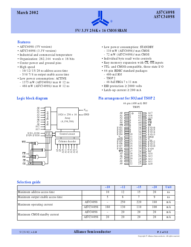
Logic block diagram
A0 A1 A2 A3 A4 A6 A7 A8 A12 A13 I/O1–I/O8 I/O9–I/O16 WE VCC 1024 × 256 × 16 Array (4,194,304) GND
Pin arrangement for SOJ and TSOP 2
44-pin (400 mil) SOJ TSOP2
Row Decoder
I/O buffer
Control circuit Column decoder A5 A9 A10 A11 A14 A15 A16 A17
UB OE LB CE
A0 A1 A2 A3 A4 CE I/O1 I/O2 I/O3 I/O4 VCC GND I/O5 I/O6 I/O7 I/O8 WE A5 A6 A7 A8 A9
1 2 3 4 5 6 7 8 9 10 11 12 13 14 15 16 17 18 19 20 21 22
44 43 42 41 40 39 38 37 36 35 34 33 32 31 30 29 28 27 26 25 24 23
A17 A16 A15 OE UB LB I/O16 I/O15 I/O14 I/O13 GND VCC I/O12 I/O11 I/O10 I/O9 NC A14 A13 A12 A11 A10
Selection guide
–10 Maximum address access time Maximum output enable access time Maximum operating current Maximum
CMOS standby...