AP60N03GS/P
Pb Free Plating Product
Advanced Power Electronics Corp.
▼ Low On-Resistance ▼ Fast Switching
www.DataSheet...
AP60N03GS/P
Pb Free Plating Product
Advanced Power Electronics Corp.
▼ Low On-Resistance ▼ Fast Switching
www.DataSheet4U.com
N-CHANNEL ENHANCEMENT MODE POWER
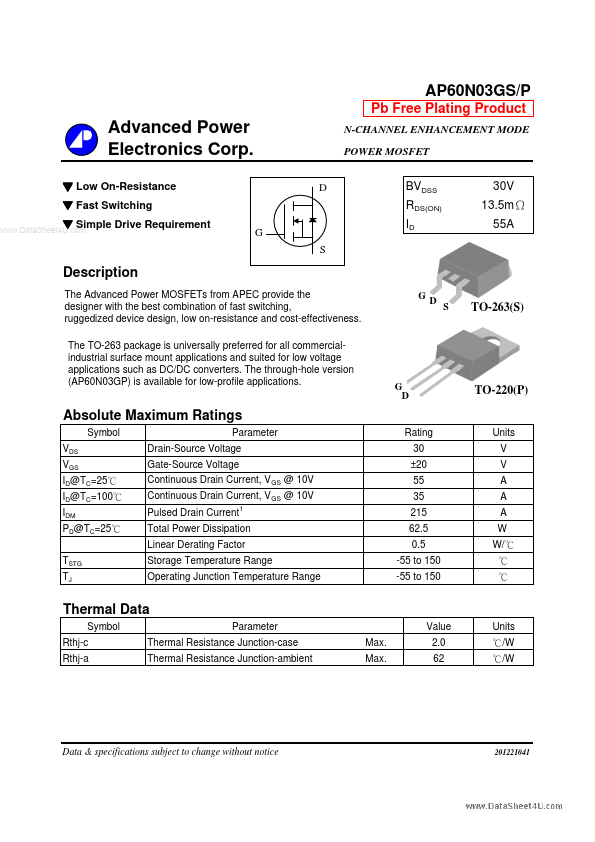
MOSFET D
BVDSS RDS(ON) ID
30V 13.5mΩ 55A
▼ Simple Drive Requirement
G S
Description
The Advanced Power
MOSFETs from APEC provide the designer with the best combination of fast switching, ruggedized device design, low on-resistance and cost-effectiveness. The TO-263 package is universally preferred for all commercialindustrial surface mount applications and suited for low
voltage applications such as DC/DC converters. The through-hole version (AP60N03GP) is available for low-profile applications. GD S
TO-263(S)
G D
TO-220(P)
Absolute Maximum Ratings
Symbol VDS VGS ID@TC=25℃ ID@TC=100℃ IDM PD@TC=25℃ TSTG TJ Parameter Drain-Source
Voltage Gate-Source
Voltage Continuous Drain Current, V GS @ 10V Continuous Drain Current, V GS @ 10V Pulsed Drain Current
1
Rating 30 ±20 55 35 215 62.5 0.5 -55 to 150 -55 to 150
Units V V A A A W W/ ℃ ℃ ℃
Total Power Dissipation Linear Derating Factor Storage Temperature Range Operating Junction Temperature Range
Thermal Data
Symbol Rthj-c Rthj-a Parameter Thermal Resistance Junction-case Thermal Resistance Junction-ambient Max. Max. Value 2.0 62 Units ℃/W ℃/W
Data & specifications subject to change without notice
201221041
AP60N03GS/P
Electrical Characteristics@Tj=25 C(unless otherwise specified)
Symbol BVDSS
ΔBVDSS/ΔTj
o
Parameter Drain-Source Breakdown
Voltage
Test Condi...