www.datasheet4u.com
AOT462 N-Channel Enhancement Mode Field Effect Transistor
Features
VDS (V) = 60V ID = 70A RDS(ON) <...
www.datasheet4u.com
AOT462 N-Channel Enhancement Mode Field Effect Transistor
Features
VDS (V) = 60V ID = 70A RDS(ON) < 18mΩ (V GS = 10V) (VGS = 10V)
General Description
The AOT462 uses advanced trench technology and design to provide excellent R DS(ON) with low gate charge. This device is suitable for use in UPS, high current switching applications. Standard Product AOT462 is Pb-free (meets ROHS & Sony 259 specifications).
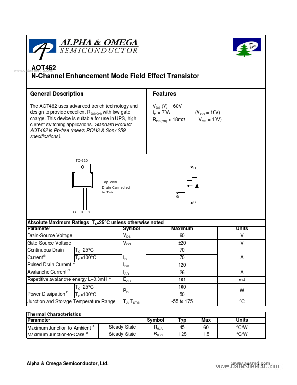
TO-220 D
Top View Drain Connected to Tab
G S
G
D
S
Absolute Maximum Ratings TA=25°C unless otherwise noted Parameter Symbol VDS Drain-Source
Voltage VGS Gate-Source
Voltage Continuous Drain CurrentG Pulsed Drain Current Avalanche Current C Repetitive avalanche energy L=0.3mH C TC=25°C Power Dissipation
B C
Maximum 60 ±20 70 70 120 26 101 100 50 -55 to 175
Units V V A A mJ W °C
TC=25°C TC=100°C ID IDM IAR EAR PD TJ, TSTG
TC=100°C
Junction and Storage Temperature Range Thermal Characteristics Parameter Maximum Junction-to-Ambient Maximum Junction-to-Case B
A
Steady-State Steady-State
Symbol RθJA RθJC
Typ 45 1.25
Max 60 1.5
Units °C/W °C/W
Alpha & Omega Semiconductor, Ltd.
www.aosmd.com
AOT462
Electrical Characteristics (TJ=25°C unless otherwise noted) Symbol
www.datasheet4u.com
Parameter
Conditions ID=250uA, VGS=0V VDS=60V, VGS=0V TJ=55°C VDS=0V, VGS=±20V VDS=VGS, ID=250µA VGS=10V, VDS=5V VGS=10V, ID=30A TJ=125°C VDS=5V, ID=30A
Min 60
Typ
Max
Units V
STATIC PARAMETERS BVDSS Drain-Source Breakdown
Voltage IDSS IGSS Zero Gate Volt...