www.datasheet4u.com
AOT430 N-Channel Enhancement Mode Field Effect Transistor
Features
VDS (V) = 75V ID = 80 A (VGS = 1...
www.datasheet4u.com
AOT430 N-Channel Enhancement Mode Field Effect Transistor
Features
VDS (V) = 75V ID = 80 A (VGS = 10V) RDS(ON) < 11.5mΩ (VGS = 10V)
General Description
The AOT430 uses advanced trench technology and design to provide excellent RDS(ON) with low gate charge. This device is suitable for use in PWM, load switching and general purpose applications. Standard Product AOT430 is Pb-free (meets ROHS & Sony 259 specifications).
UIS TESTED!
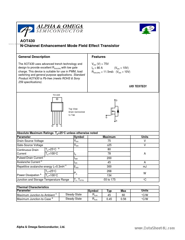
TO-220 D
Top View Drain Connected to Tab
G S
G
D
S
Absolute Maximum Ratings TA=25°C unless otherwise noted Parameter Symbol VDS Drain-Source
Voltage VGS Gate-Source
Voltage Continuous Drain Current Pulsed Drain Current Avalanche Current
C C C
Maximum 75 ±25 80 78 200 45 300 268 134 -55 to 175
Units V V A A mJ W °C
TC=25°C TC=100°C
G
ID IDM IAR EAR PD TJ, TSTG
Repetitive avalanche energy L=0.3mH TC=25°C Power Dissipation B TC=100°C
Junction and Storage Temperature Range Thermal Characteristics Parameter Maximum Junction-to-Ambient A Maximum Junction-to-Case B
Steady-State Steady-State
Symbol RθJA RθJC
Typ 45 0.45
Max 60 0.56
Units °C/W °C/W
Alpha & Omega Semiconductor, Ltd.
AOT430
Electrical Characteristics (T J=25°C unless otherwise noted) Parameter Symbol STATIC PARAMETERS BVDSS Drain-Source Breakdown
Voltage www.datasheet4u.com IDSS IGSS VGS(th) ID(ON) RDS(ON) gFS VSD IS Zero Gate
Voltage Drain Current Gate-Body leakage current Gate Threshold
Voltage On state drain current Static Drain-Source On-Resistance...