AON6405L P-Channel Enhancement Mode Field Effect Transistor
General Description
The AON6405L combines advanced trench MO...
AON6405L P-Channel Enhancement Mode Field Effect Transistor
General Description
The AON6405L combines advanced trench
MOSFET technology with a low resistance package to provide extremely low RDS(ON).This device is ideal for load switch and battery protection applications.
Features
VDS (V) = -30V (VGS = -10V) ID = -30A RDS(ON) < 7mΩ (VGS = -10V) RDS(ON) < 8mΩ (VGS = -4.5V) ESD Protected! 100% UIS Tested!
-RoHS Compliant -Halogen Free
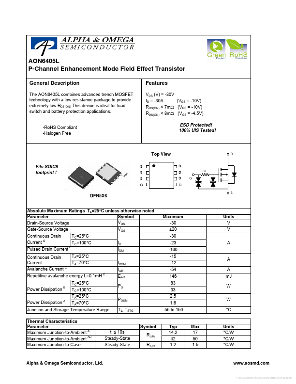
Top View Fits SOIC8 footprint !
S S S G D D D D G
Rg
D
DFN5X6 Absolute Maximum Ratings TA=25°C unless otherwise noted Parameter Symbol VDS Drain-Source
Voltage VGS Gate-Source
Voltage Continuous Drain G Current Pulsed Drain Current Continuous Drain Current Avalanche Current
C C
S
Maximum -30 ±20 -30 -23 -160 -15 -12 -54 146 83 33 2.5 1.6 -55 to 150
Units V V A
TC=25°C TC=100°C TA=25°C TA=70°C
C
ID IDM IDSM IAR EAR PD PDSM TJ, TSTG
A A mJ W W °C
Repetitive avalanche energy L=0.1mH Power Dissipation
B
TC=25°C TC=100°C TA=25°C TA=70°C
Power Dissipation A
Junction and Storage Temperature Range Thermal Characteristics Parameter A Maximum Junction-to-Ambient Maximum Junction-to-Ambient AD Maximum Junction-to-Case
Symbol t ≤ 10s Steady-State Steady-State RθJA RθJC
Typ 14.2 42 1.2
Max 17 50 1.5
Units °C/W °C/W °C/W
Alpha & Omega Semiconductor, Ltd.
www.aosmd.com
Free Datasheet http://www.datasheet4u.com/
AON6405L
Electrical Characteristics (TJ=25°C unless otherwise noted) Symbol Parameter Conditions ID=-250µA, VGS=0V VDS=-30V, VGS=...