AOD4185/AOI4185 P-Channel Enhancement Mode Field Effect Transistor
General Description
The AOD4185/AOI4185 uses advanced...
AOD4185/AOI4185 P-Channel Enhancement Mode Field Effect Transistor
General Description
The AOD4185/AOI4185 uses advanced trench technology to provide excellent RDS(ON) and low gate charge. With the excellent thermal resistance of the DPAK/IPAK package, this device is well suited for high current applications. -RoHS Compliant -Halogen Free*
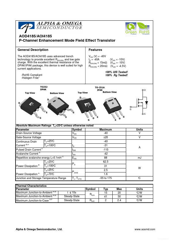
TO252 DPAK Top View D D D G S G S G G D S S D G S Bottom View Top View D
Features
VDS (V) = -40V ID = -40A (VGS = -10V) RDS(ON) < 15mΩ (VGS = -10V) RDS(ON) < 20mΩ (VGS = -4.5V) 100% UIS Tested! 100% Rg Tested!
TO-251A IPAK Bottom View
D
Absolute Maximum Ratings TC=25° C unless otherwise noted Parameter Symbol Drain-Source
Voltage VDS Gate-Source
Voltage Continuous Drain Current B,H Pulsed Drain Current Avalanche Current C Repetitive avalanche energy L=0.1mH TC=25° C Power Dissipation B Power Dissipation A TC=100° C TA=25° C TA=70° C Junction and Storage Temperature Range Thermal Characteristics Parameter Maximum Junction-to-Ambient A,G Maximum Junction-to-Ambient A,G Maximum Junction-to-Case
D,F C C
Maximum -40 ±20 -40 -31 -115 -42 88 62.5 31 2.5 1.6 -55 to 175
Units V V
VGS TC=25° C TC=100° C ID IDM IAR EAR PD PDSM TJ, TSTG
A
mJ
W
° C
Symbol t ≤ 10s Steady-State Steady-State RθJA RθJC
Typ 15 41 2
Max 20 50 2.4
Units ° C/W ° C/W ° C/W
Alpha & Omega Semiconductor, Ltd.
www.aosmd.com
Free Datasheet http://www.datasheet4u.com/
AOD4185/AOI4185
Electrical Characteristics (TJ=25° C unless otherwise noted) Symbol Parameter Cond...