AOD4102/AOI4102
30V N-Channel MOSFET
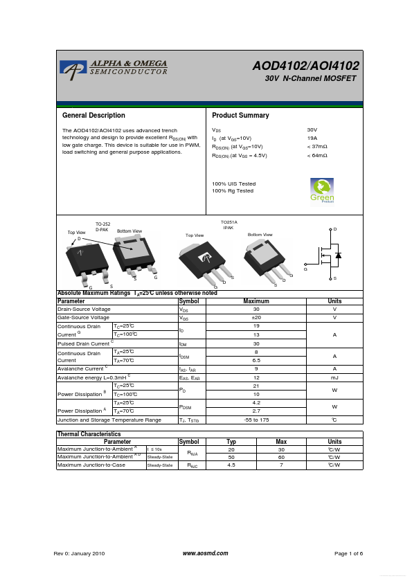
General Description
The AOD4102/AOI4102 uses advanced trench technology and design...
AOD4102/AOI4102
30V N-Channel
MOSFET
General Description
The AOD4102/AOI4102 uses advanced trench technology and design to provide excellent RDS(ON) with low gate charge. This device is suitable for use in PWM, load switching and general purpose applications.
Product Summary
VDS ID (at VGS=10V) RDS(ON) (at VGS=10V) RDS(ON) (at VGS = 4.5V) 30V 19A < 37mΩ < 64mΩ
100% UIS Tested 100% Rg Tested
Top View D
TO-252 D-PAK
Bottom View
TO251A IPAK Top View Bottom View
D
G S G S G D G S S G D S
Absolute Maximum Ratings TA=25° C unless otherwise noted Parameter Symbol Drain-Source
Voltage VDS Gate-Source
Voltage Continuous Drain Current G Pulsed Drain Current C Continuous Drain Current Avalanche Current
C C
Maximum 30 ±20 19 13 30 8 6.5 9 12 21 10 4.2 2.7 -55 to 175
Units V V A
VGS TC=25° C TC=100° C TA=25° C TA=70° C ID IDM IDSM IAS, IAR EAS, EAR PD PDSM TJ, TSTG
A A mJ W W ° C
Avalanche energy L=0.3mH TC=25° C Power Dissipation B Power Dissipation A TC=100° C TA=25° C TA=70° C Junction and Storage Temperature Range Thermal Characteristics Parameter Maximum Junction-to-Ambient A Maximum Junction-to-Ambient A D Maximum Junction-to-Case
Symbol
t ≤ 10s Steady-State Steady-State
RθJA RθJC
Typ 20 50 4.5
Max 30 60 7
Units ° C/W ° C/W ° C/W
Rev 0: January 2010
www.aosmd.com
Page 1 of 6
Free Datasheet http://www.datasheet4u.com/
AOD4102/AOI4102
Electrical Characteristics (TJ=25° C unless otherwise noted) Symbol Parameter Conditions ID=250µA, VGS=0V VDS=30V, VGS=0V TJ=5...