isc N-Channel MOSFET Transistor
AOD8N25
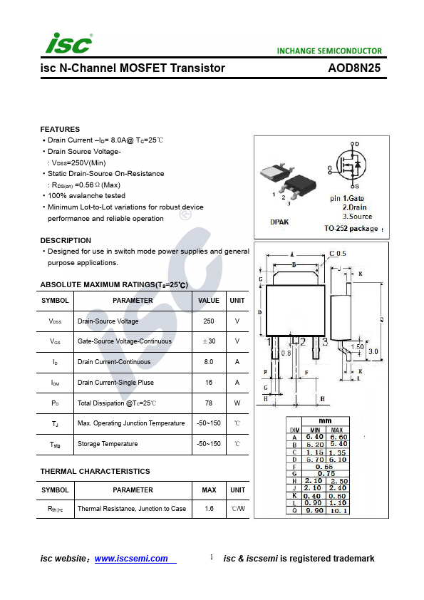
FEATURES ·Drain Current –ID= 8.0A@ TC=25℃ ·Drain Source Voltage-
: VDSS=250V(M...
isc N-Channel
MOSFET Transistor
AOD8N25
FEATURES ·Drain Current –ID= 8.0A@ TC=25℃ ·Drain Source
Voltage-
: VDSS=250V(Min) ·Static Drain-Source On-Resistance
: RDS(on) =0.56Ω(Max) ·100% avalanche tested ·Minimum Lot-to-Lot variations for robust device
performance and reliable operation
DESCRIPTION ·Designed for use in switch mode power supplies and general
purpose applications.
ABSOLUTE MAXIMUM RATINGS(Ta=25℃)
SYMBOL
PARAMETER
VALUE UNIT
VDSS
Drain-Source
Voltage
250
V
VGS
Gate-Source
Voltage-Continuous
±30
V
ID
Drain Current-Continuous
8.0
A
IDM
Drain Current-Single Pluse
16
A
PD
Total Dissipation @TC=25℃
78
W
TJ
Max. Operating Junction Temperature -50~150 ℃
Tstg
Storage Temperature
-50~150 ℃
THERMAL CHARACTERISTICS
SYMBOL
PARAMETER
Rth j-c Thermal Resistance, Junction to Case
MAX UNIT
1.6
℃/W
isc website:www.iscsemi.com
1 isc & iscsemi is registered trademark
isc N-Channel
MOSFET Transistor
AOD8N25
ELECTRICAL CHARACTERISTICS
TC=25℃ unless otherwise specified
SYMBOL
PARAMETER
CONDITIONS
V(BR)DSS Drain-Source Breakdown
Voltage
VGS= 0; ID= 0.25mA
VGS(th) Gate Threshold
Voltage
VDS= VGS; ID= 0.25mA
RDS(on) Drain-Source On-Resistance
VGS= 10V; ID=1.5A
IGSS
Gate-Body Leakage Current
IDSS
Zero Gate
Voltage Drain Current
VSD
Forward On-
Voltage
VGS= ±30V;VDS= 0
VDS=250V; VGS= 0 VDS=200V; VGS= 0@TJ=125℃
IS= 1A; VGS= 0
MIN MAX UNIT
250
V
3.1
4.3
V
0.56
Ω
±100 nA
1 10
μA
1.0
V
NOTICE: ISC reserves the rights to ma...