AO6401A P-Channel Enhancement Mode Field Effect Transistor
General Description
The AO6401A uses advanced trench technolo...
AO6401A P-Channel Enhancement Mode Field Effect Transistor
General Description
The AO6401A uses advanced trench technology to provide excellent RDS(ON), low gate charge and www.DataSheet4U.com operation with gate
voltages as low as 2.5V. This device is suitable for use as a load switch or in PWM applications. AO6401A is Pb-free (meets ROHS & Sony 259 specifications).
Features
VDS = -30V ID = -5.0A RDS(ON) < 44mΩ RDS(ON) < 55mΩ RDS(ON) < 82mΩ (VGS = -10V) (VGS = -10V) (VGS = -4.5V) (VGS = -2.5V)
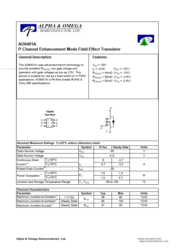
D TSOP6 Top View D D G 1 6 2 5 3 4 D D S G S
Absolute Maximum Ratings TA=25°C unless otherwise noted Symbol 10 Sec Steady State Parameter Drain-Source
Voltage VDS -30 Gate-Source
Voltage Continuous Drain A Current Pulsed Drain Current Power Dissipation
A B
Units V V
VGS TA=25°C TA=70°C TA=25°C TA=70°C ID IDM PD TJ, TSTG 1.6 1.0 -5 -3.7
±12 -3.7 -3.2 -25 1.0 0.7 -55 to 150
A
W °C
Junction and Storage Temperature Range Thermal Characteristics Parameter A Maximum Junction-to-Ambient A Maximum Junction-to-Ambient Maximum Junction-to-Lead
C
Symbol t ≤ 10s Steady State Steady State RθJA RθJL
Typ 58 94 37
Max 80 120 50
Units °C/W °C/W °C/W
Alpha & Omega Semiconductor, Ltd.
www.aosmd.com
AO6401A
Electrical Characteristics (TJ=25°C unless otherwise noted) Parameter Symbol STATIC PARAMETERS BVDSS Drain-Source Breakdown
Voltage IDSS IGSS VGS(th) ID(ON)
www.DataSheet4U.com
Conditions ID = -250µA, VGS = 0V VDS = -30V, VGS = 0V TJ = 55°C VDS = 0V, VGS = ±12V VDS = VGS ID = -250µA V...