AO4812A Dual N-Channel Enhancement Mode Field Effect Transistor
General Description
The AO4812A uses advanced trench tec...
AO4812A Dual N-Channel Enhancement Mode Field Effect Transistor
General Description
The AO4812A uses advanced trench technology to provide excellent RDS(ON) and low gate charge. The two
MOSFETs make a compact and efficient switch and synchronous rectifier combination for use in buck converters. AO4812A is Pb-free (meets ROHS & Sony 259 specifications). AO4812AL is a Green Product ordering option. AO4812A and AO4812AL are electrically identical.
Features
VDS (V) = 30V ID = 6.9A (VGS = 10V) RDS(ON) < 28m Ω (VGS = 10V) RDS(ON) < 42m Ω (VGS = 4.5V)
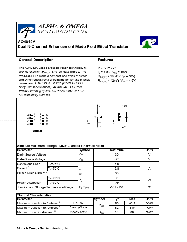
D1 S2 G2 S1 G1 D2 D2 D1 D1
D2
www.DataSheet4U.com
1 2 3 4
8 7 6 5
G1 S1
G2 S2
SOIC-8
Absolute Maximum Ratings TA=25°C unless otherwise noted Parameter Symbol VDS Drain-Source
Voltage Gate-Source
Voltage Continuous Drain Current A Pulsed Drain Current Power Dissipation
B
Maximum 30 ±20 6.9 5.8 30 2 1.44 -55 to 150
Units V V A
VGS TA=25°C TA=70°C TA=25°C TA=70°C ID IDM PD TJ, TSTG
W °C
Junction and Storage Temperature Range Thermal Characteristics Parameter Maximum Junction-to-Ambient A Maximum Junction-to-Ambient A Maximum Junction-to-Lead C
Symbol t ≤ 10s Steady-State Steady-State RθJA RθJL
Typ 50 82 41
Max 62.5 110 50
Units °C/W °C/W °C/W
Alpha & Omega Semiconductor, Ltd.
AO4812A
Electrical Characteristics (T J=25°C unless otherwise noted) Symbol Parameter Conditions ID=250µA, VGS=0V VDS=24V, VGS=0V TJ=55°C VDS=0V, VGS= ±20V VDS=VGS ID=250µA VGS=4.5V, VDS=5V VGS=10V, ID=6.9A RDS(ON) gFS VSD IS Static Drain-Source...