AO4709 P-Channel Enhancement Mode Field Effect Transistor with Schottky Diode
General Description
The AO4709 uses advanc...
AO4709 P-Channel Enhancement Mode Field Effect Transistor with Schottky Diode
General Description
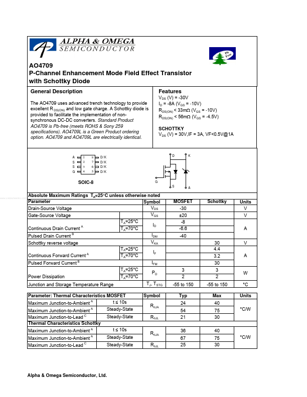
The AO4709 uses advanced trench technology to provide excellent R DS(ON) and low gate charge. A Schottky diode is provided to facilitate the implementation of nonsynchronous DC-DC converters. Standard Product AO4709 is Pb-free (meets ROHS & Sony 259 specifications). AO4709L is a Green Product ordering option. AO4709 and AO4709L are electrically identical.
Features
VDS (V) = -30V ID = -8A (VGS = -10V) RDS(ON) < 33mΩ (VGS = -10V) RDS(ON) < 56mΩ (VGS = -4.5V) SCHOTTKY VDS (V) = 30V,IF = 3A, VF<0.5V@1A
A S S G
1 2 3 4
8 7 6 5
D/K D/K D/K D/K G
D
K
SOIC-8
S
A
www.DataSheet4U.com
Absolute Maximum Ratings TA=25°C unless otherwise noted Parameter Symbol VDS Drain-Source
Voltage Gate-Source
Voltage TA=25°C Continuous Drain Current Pulsed Drain Current
B A
MOSFET -30 ±20 -8 -6.6 -40
Schottky
Units V V A
VGS TA=70°C ID IDM VKA TA=25°C
A
Schottky reverse
voltage Continuous Forward Current Pulsed Forward Current Power Dissipation Junction and Storage Temperature Range Parameter: Thermal Characteristics
MOSFET t ≤ 10s Maximum Junction-to-Ambient A Maximum Junction-to-Ambient A Maximum Junction-to-Lead Thermal Characteristics Schottky Maximum Junction-to-Ambient Maximum Junction-to-Ambient Maximum Junction-to-Lead C
A A C B
TA=70°C TA=25°C TA=70°C
IF IFM PD TJ, TSTG Symbol RθJA RθJL RθJA RθJL 3 2 -55 to 150 Typ 24 54 21 36 67 25
30 4.4 3.2 30 3 2 -55 to 150 Max 40 75 30 40 7...