AO4601 Complementary Enhancement Mode Field Effect Transistor
General Description
The AO4601 uses advanced trench techno...
AO4601 Complementary Enhancement Mode Field Effect Transistor
General Description
The AO4601 uses advanced trench technology
MOSFETs to provide excellent RDS(ON) and low gate charge. The complementary
MOSFETs may be used to form a level shifted high side switch, and for a host of other applications. Standard Product AO4601 is Pb-free (meets ROHS & Sony 259 specifications). AO4601L is a Green Product ordering option. AO4601 and AO4601L are n-channel p-channel -30V VDS (V) = 30V ID = 4.7A (VGS=10V) -8A (VGS = -20V) RDS(ON) RDS(ON) < 55m Ω (VGS=10V) < 18mΩ (VGS = -20V) < 70m Ω (VGS=4.5V) < 19mΩ (VGS = -10V) < 110m Ω (VGS = 2.5V)
Features
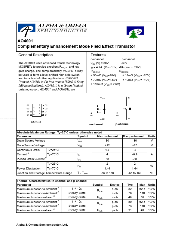
D2 S2 G2 S1 G1
www.DataSheet4U.com
D1
1 2 3 4
8 7 6 5
D2 D2 D1 D1
G2 S2
G1 S1
SOIC-8
n-channel
p-channel
Absolute Maximum Ratings TA=25°C unless otherwise noted Parameter Max n-channel Symbol VDS Drain-Source
Voltage 30 Gate-Source
Voltage Continuous Drain Current A Pulsed Drain Current Power Dissipation
B
Max p-channel -30 ±25 -8 -6.9 -50 2 1.44 -55 to 150
Units V V A
VGS TA=25°C TA=70°C TA=25°C TA=70°C ID IDM PD TJ, TSTG
±12 4.7 4 30 2 1.44 -55 to 150
W °C
Junction and Storage Temperature Range
Thermal Characteristics: n-channel and p-channel Parameter t ≤ 10s Maximum Junction-to-Ambient A A Steady-State Maximum Junction-to-Ambient C Steady-State Maximum Junction-to-Lead A t ≤ 10s Maximum Junction-to-Ambient A Steady-State Maximum Junction-to-Ambient Steady-State Maximum Junction-to-Lead C
Symbol RθJA RθJL RθJA RθJL
Device...